SNOSD45B February   2018  – October 2018 LMG1020

PRODUCTION DATA.  

  1. Features
  2. Applications
  3. Description
    1.     Device Images
      1.      Simplified LiDAR Driver Stage Diagram
  4. Revision History
  5. Pin Configuration and Functions
    1.     Pin Functions
  6. Specifications
    1. 6.1 Absolute Maximum Ratings
    2. 6.2 ESD Ratings
    3. 6.3 Recommended Operating Conditions
    4. 6.4 Thermal Information
    5. 6.5 Electrical Characteristics
    6. 6.6 Switching Characteristics
    7. 6.7 Typical Characteristics
  7. Detailed Description
    1. 7.1 Overview
    2. 7.2 Functional Block Diagram
    3. 7.3 Feature Description
      1. 7.3.1 Input Stage
      2. 7.3.2 Output Stage
      3. 7.3.3 VDD and undervoltage lockout
      4. 7.3.4 Overtemperature Protection (OTP)
    4. 7.4 Device Functional Modes
  8. Application and Implementation
    1. 8.1 Application Information
    2. 8.2 Typical Application
      1. 8.2.1 Design Requirements
      2. 8.2.2 Detailed Design Procedure
        1. 8.2.2.1 Handling Ground Bounce
        2. 8.2.2.2 Creating Nanosecond Pulse With LMG1020
      3. 8.2.3 VDD and Overshoot
      4. 8.2.4 Operating at Higher Frequency
      5. 8.2.5 Application Curves
  9. Power Supply Recommendations
  10. 10Layout
    1. 10.1 Layout Guidelines
      1. 10.1.1 Gate Drive Loop Inductance and Ground Connection
      2. 10.1.2 Bypass Capacitor
    2. 10.2 Layout Example
  11. 11Device and Documentation Support
    1. 11.1 Documentation Support
      1. 11.1.1 Related Documentation
    2. 11.2 Receiving Notification of Documentation Updates
    3. 11.3 Community Resources
    4. 11.4 Trademarks
    5. 11.5 Electrostatic Discharge Caution
    6. 11.6 Glossary
  12. 12Mechanical, Packaging, and Orderable Information

Package Options

Mechanical Data (Package|Pins)
Thermal pad, mechanical data (Package|Pins)
Orderable Information

Pin Configuration and Functions

YFF Package
6-Ball WCSP
Top View
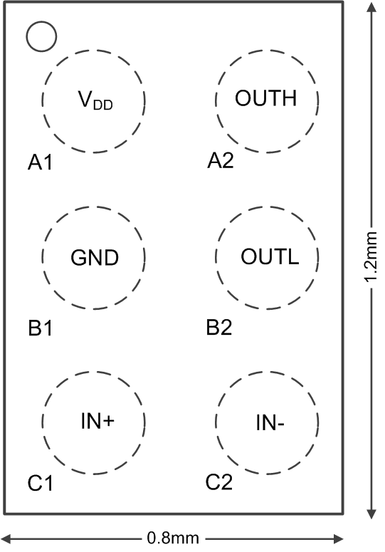
LMG1020 lmg1020-package-top-view-snosd45.gif

Pin Functions

PIN I/O DESCRIPTION
NAME NO.
GND B1 Ground
IN+ C1 I Positive logic-level input
IN– C2 I Negative logic-level input
OUTL B2 O Pulldown gate drive output. Connect through an optional resistor to the target transistor’s gate
OUTH A2 O Pullup gate drive output. Connect through a resistor to the target transistor’s gate
VDD A1 I Input voltage supply. Decouple through a small size, low inductance capacitor to GND