SNOSD74B May 2019 – January 2020 LMG1025-Q1
PRODUCTION DATA.
- 1 Features
- 2 Applications
- 3 Description
- 4 Revision History
- 5 Pin Configuration and Functions
- 6 Specifications
- 7 Detailed Description
- 8 Application and Implementation
- 9 Power Supply Recommendations
- 10Layout
- 11Device and Documentation Support
- 12Mechanical, Packaging, and Orderable Information
Package Options
Mechanical Data (Package|Pins)
- DEE|6
Thermal pad, mechanical data (Package|Pins)
Orderable Information
8.2.5 Application Curves
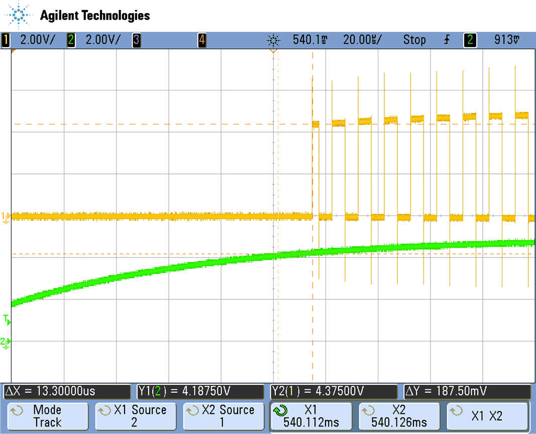
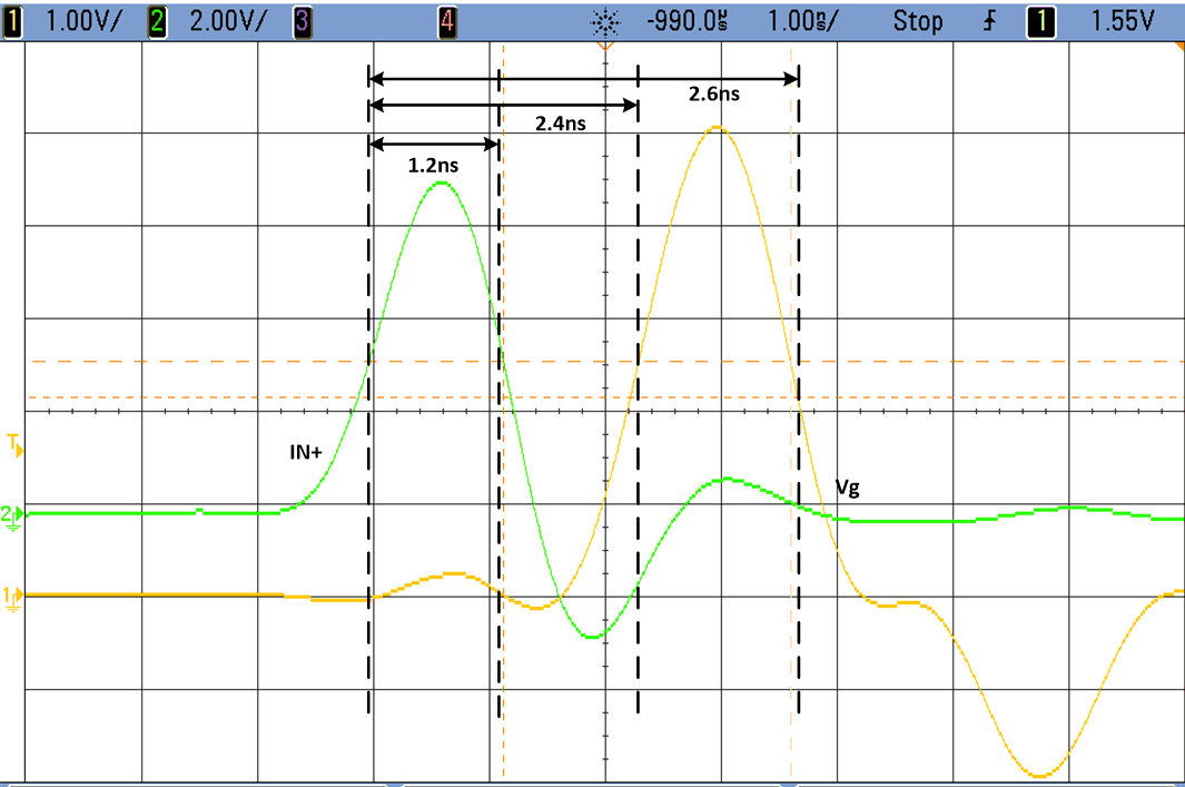
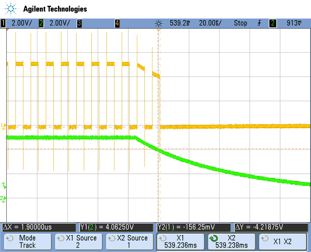
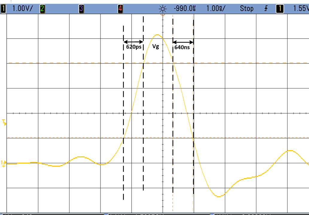
LMG1025-Q1 EVM is used to take application waveforms. This EVM has LDO, input buffer, GaN FET, and load resistor. It shows the switching performance of the LMG1025-Q1 when equivalent laser diode current is switched. Figure 11 and Figure 12 show VDD turn-on and turn-off delay in an application-like set-up. System designer need to make sure that these delays are acceptable in their designs. LIDAR design needs to pulse the laser diode for very short duration. Figure 13 shows how LMG1025-Q1 can not only handle nano-second pulse at its input but also can produce a nano-second pulse at the output while driving a reasonably sized GaN FET that has 3.2nC of typical total gate charge. Figure 13 also shows very small, e.g. less than 3 ns, rising and falling propagation delay of LMG1025-Q1. Figure 14 shows drive strength of LMG1025-Q1. It shows how LMG1025-Q1 can achieve sub-nano second rise and fall time, which is very important for LIDAR applicatoins.
 Figure 11. Startup Time
  Figure 13. Input pulse width and propagation delays
  Figure 12. Shutdown Time
  Figure 14. Rise and fall time