SNOSD74B May 2019 – January 2020 LMG1025-Q1
PRODUCTION DATA.
- 1 Features
- 2 Applications
- 3 Description
- 4 Revision History
- 5 Pin Configuration and Functions
- 6 Specifications
- 7 Detailed Description
- 8 Application and Implementation
- 9 Power Supply Recommendations
- 10Layout
- 11Device and Documentation Support
- 12Mechanical, Packaging, and Orderable Information
Package Options
Mechanical Data (Package|Pins)
- DEE|6
Thermal pad, mechanical data (Package|Pins)
Orderable Information
8.2.2.2 Creating Nanosecond Pulse
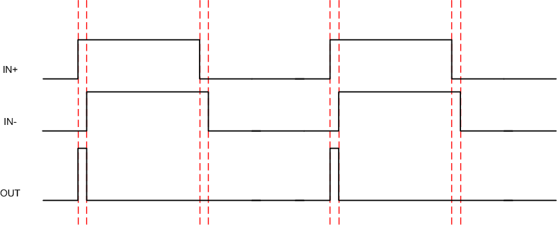
LMG1025-Q1 can be used to drive pulses of nano seconds duration on to a capacitive load. LMG1025-Q1 can be driven with a equivalently short pulse on one input pin. However, this takes a sufficiently strong digital driver and careful consideration of the routing parasitics from digital output to input of LMG1025-Q1. Two inputs and included AND gate in LMG1025-Q1 provide an alternate method to create a short pulse at the LMG1025-Q1 output. Starting with both IN+ and IN– at low, taking IN+ high will cause the output to go high. Now if IN– is taken high as well, output will be pulled low. So a digital signal and its delayed version can be applied to IN+ and IN– respectively to create a pulse at the output with width corresponding to the delay between the signals, as shown in Figure 10. The delay can be digitally controlled in the nanosecond range. This method alleviates the requirements for driving the input of LMG1025-Q1. If a separate delayed version of the digital signal is not available, an RC delay followed by a buffer can be used to derive the second signal. Optionally, if LMG1025-Q1 must be driven with a single short duration pulse, that pulse can itself be generated using another LMG1025-Q1 by the above method to meet drive requirements.
 Figure 10. Timing Diagram To Create Short Pulses