SNOSD12D November 2018 – January 2019 LMG1210
PRODUCTION DATA.
- 1 Features
- 2 Applications
- 3 Description
- 4 Revision History
- 5 Pin Configuration and Functions
- 6 Specifications
- 7 Detailed Description
- 8 Application and Implementation
- 9 Power Supply Recommendations
- 10Layout
- 11Device and Documentation Support
- 12Mechanical, Packaging, and Orderable Information
Package Options
Mechanical Data (Package|Pins)
- RVR|19
Thermal pad, mechanical data (Package|Pins)
Orderable Information
8.2.2.3 Handling Ground Bounce
For the best switching performance, it is important to connect the VSS gate return to the source of the low-side FET with a very low-inductance path.
However, doing so can cause the ground of the LMG1210 to bounce relative to the system or controller ground and cause erroneous switching transitions on the inputs. Multiple strategies can be employed to eliminate these undesired transitions.
The LMG1210 has input hysteresis built into the input buffers to help counteract this effect, but this alone may not be sufficient in all applications. The simplest option is to tie the system ground together and the power ground only at the LMG1210 (single-point connection). This gives the cleanest solution but may not always be possible depending on system grounding requirements.
For moderate ground-bounce cases, a simple R-C filter can be built with a simple resistor in series with the inputs. The resistor should be close to the inputs of the LMG1210. The input capacitance of the LMG1210 produces an RC filter which can help decrease ringing at the inputs. The addition of a small C on the inputs to supplement the LMG1210 input capacitance can also be helpful. This solution is acceptable for moderate cases in applications where the extra delay is acceptable.
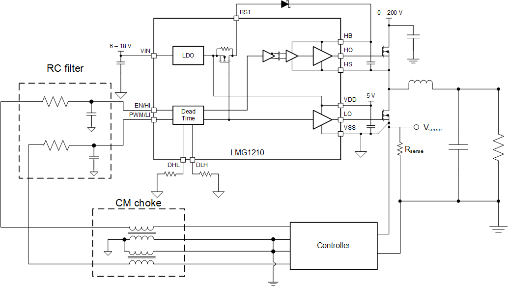
For more extreme cases or where no delay is tolerable, using a common-mode choke provides the best results. One example application where the ground bounce is particularly challenging is when using a current sense resistor. In this application, the LMG1210 ground is connected to the GaN source, while the controller ground is connected to the other side of the current sense resistor as shown in Figure 18.
 Figure 18. LMG1210 Configured With Current Sense Resistor Using a CMC as Filter
 The combination of high dI/dt experienced through the sense resistor inductance will cause severe ground noise that could cause false triggering or even damage the part. To prevent this, a common-mode choke (CMC) can be used. Each signal requires its own CMC. Also, to provide additional RC filtering, a 100 Ω resistor should be added to the signal output line before the LMG1210.