SNOSD12D November 2018 – January 2019 LMG1210
PRODUCTION DATA.
- 1 Features
- 2 Applications
- 3 Description
- 4 Revision History
- 5 Pin Configuration and Functions
- 6 Specifications
- 7 Detailed Description
- 8 Application and Implementation
- 9 Power Supply Recommendations
- 10Layout
- 11Device and Documentation Support
- 12Mechanical, Packaging, and Orderable Information
Package Options
Mechanical Data (Package|Pins)
- RVR|19
Thermal pad, mechanical data (Package|Pins)
Orderable Information
6.7 Typical Characteristics
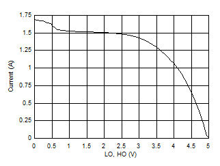 Figure 1. Peak Source Current vs Output Voltage
 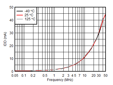 Figure 3. IDD vs Frequency, Unloaded
 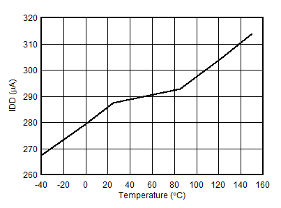 Figure 5. IDD vs Temperature
 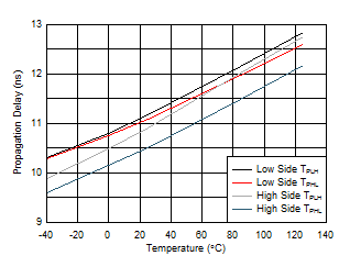 Figure 7. Propagation Delay vs Temperature
 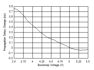 Figure 9. Propagation Delay Change vs Bootstrap voltage
 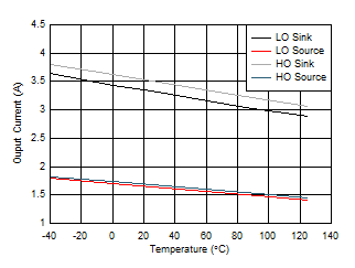 Figure 11. LO and HO Output Current vs Temperature
 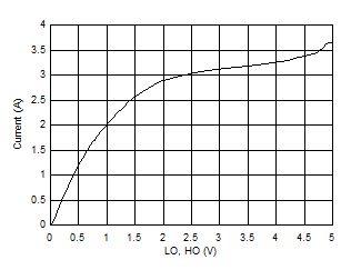 Figure 2. Peak Sink Current vs Output Voltage
 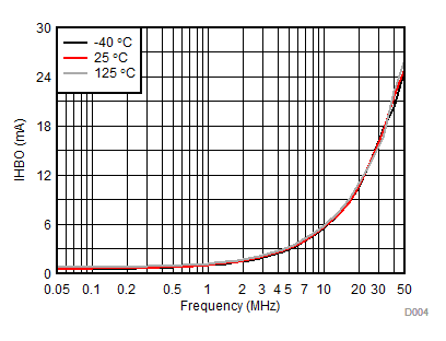 Figure 4. IHBO vs Frequency, Unloaded
 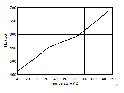 Figure 6. IHB vs Temperature
 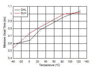 Figure 8. Minimum Dead Time vs Temperature
 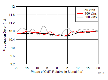 Figure 10. Propagation Delay vs relative phase of CMTI Phase
 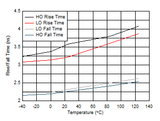 Figure 12. 1 nF Loaded Rise and Fall Time vs Temperature