SNOSD81B September 2018 – January 2020 LMG3410R050 , LMG3411R050
PRODUCTION DATA.
- 1 Features
- 2 Applications
- 3 Description
- 4 Revision History
- 5 Pin Configuration and Functions
- 6 Specifications
- 7 Parameter Measurement Information
-
8 Detailed Description
- 8.1 Overview
- 8.2 Functional Block Diagram
- 8.3 Feature Description
- 8.4 Safe Operation Area (SOA)
- 9 Application and Implementation
- 10Power Supply Recommendations
- 11Layout
- 12Device and Documentation Support
- 13Mechanical, Packaging, and Orderable Information
Package Options
Mechanical Data (Package|Pins)
- RWH|32
Thermal pad, mechanical data (Package|Pins)
Orderable Information
10.2.2 Managing the Bootstrap Voltage
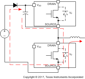
In a synchronous buck, totem-pole PFC, or other converter where the low-side switch occasionally operates in third-quadrant mode, it is important to consider the bootstrap supply. During the dead time, the bootstrap supply charges through a path that includes the third-quadrant voltage drop of the low-side LMG341xR050. This third-quadrant drop can be large, which may over-charge the bootstrap supply in certain conditions. The VDD supply of LMG341xR050 must not exceed 18 V in bootstrap operation.
 Figure 22. Charging Path for Bootstrap Diode
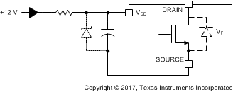
 The recommended bootstrap supply connection includes a bootstrap diode and a series resistor with an optional zener as shown in Figure 23. The series resistor limits the charging current at startup and when the low-side device is operating in third-quadrant mode. This resistor must be chosen to allow sufficient current to power the LMG341xR050 at the desired operating frequency. At 100 kHz operation, a value of approximately 5.1 Ω is recommended. At higher frequencies, this resistor value should be reduced or the resistor omitted entirely to ensure sufficient supply current.
 Figure 23. Suggested Bootstrap Regulation Circuit
 Using a series resistor with the bootstrap supply will create a charging time constant in conjunction with the bypass capacitance on the order of a microsecond. When the dead time, or third-quadrant conduction time, is much lower than this time constant, the bootstrap voltage will be well-controlled and the optional zener clamp in Figure 23 will not be necessary. If a large deadtime is needed, a 14-V zener diode can be used in parallel with the VDD bypass capacitor to prevent damaging the high-side LMG341xR050.