SNOSD91B March   2019  – February 2020 LMG3410R150 , LMG3411R150

PRODUCTION DATA.  

  1. Features
  2. Applications
  3. Description
    1.     Device Images
      1.      Simplified Block Diagram
      2.      Switching Performance
  4. Revision History
  5. Pin Configuration and Functions
    1.     Pin Functions
  6. Specifications
    1. 6.1 Absolute Maximum Ratings
    2. 6.2 ESD Ratings
    3. 6.3 Recommended Operating Conditions
    4. 6.4 Thermal Information
    5. 6.5 Electrical Characteristics
    6. 6.6 Switching Characteristics
    7. 6.7 Typical Characteristics
  7. Parameter Measurement Information
    1. 7.1 Switching Parameters
    2. 7.2 Turn-on Delays
    3. 7.3 Turn-off Delays
    4. 7.4 Drain Slew Rate
  8. Detailed Description
    1. 8.1 Overview
    2. 8.2 Functional Block Diagram
    3. 8.3 Feature Description
      1. 8.3.1 Direct-Drive GaN Architecture
      2. 8.3.2 Internal Buck-Boost DC-DC Converter
      3. 8.3.3 Internal Auxiliary LDO
      4. 8.3.4 Start Up Sequence
      5. 8.3.5 R-C Decoupling for IN pin
      6. 8.3.6 Low Power Mode
      7. 8.3.7 Fault Detection
        1. 8.3.7.1 Overcurrent Protection
        2. 8.3.7.2 Over-Temperature Protection and UVLO
      8. 8.3.8 Drive Strength Adjustment
    4. 8.4 Safe Operation Area (SOA)
      1. 8.4.1 Repetitive SOA
  9. Application and Implementation
    1. 9.1 Application Information
    2. 9.2 Typical Application
      1. 9.2.1 Design Requirements
      2. 9.2.2 Detailed Design Procedure
        1. 9.2.2.1 Slew Rate Selection
          1. 9.2.2.1.1 Startup and Slew Rate with Bootstrap High-Side Supply
        2. 9.2.2.2 Signal Level-Shifting
        3. 9.2.2.3 Buck-Boost Converter Design
    3. 9.3 Dos and Don'ts
  10. 10Power Supply Recommendations
    1. 10.1 Using an Isolated Power Supply
    2. 10.2 Using a Bootstrap Diode
      1. 10.2.1 Diode Selection
      2. 10.2.2 Managing the Bootstrap Voltage
      3. 10.2.3 Reliable Bootstrap Start-up
  11. 11Layout
    1. 11.1 Layout Guidelines
      1. 11.1.1 Power Loop Inductance
      2. 11.1.2 Signal Ground Connection
      3. 11.1.3 Bypass Capacitors
      4. 11.1.4 Switch-Node Capacitance
      5. 11.1.5 Signal Integrity
      6. 11.1.6 High-Voltage Spacing
      7. 11.1.7 Thermal Recommendations
    2. 11.2 Layout Example
  12. 12Device and Documentation Support
    1. 12.1 Device Support
      1. 12.1.1 Third-Party Products Disclaimer
    2. 12.2 Documentation Support
      1. 12.2.1 Related Documentation
    3. 12.3 Receiving Notification of Documentation Updates
    4. 12.4 Community Resources
    5. 12.5 Trademarks
    6. 12.6 Electrostatic Discharge Caution
    7. 12.7 Glossary
  13. 13Mechanical, Packaging, and Orderable Information

Package Options

Mechanical Data (Package|Pins)
Thermal pad, mechanical data (Package|Pins)
Orderable Information

Repetitive SOA

The allowed repetitive SOA for the LMG341xR150 (Figure 12) is defined by the peak drain current (IDS) and the drain to source voltage (VDS) of the device during turn on. The peak drain current during switching is the sum of several currents going into drain terminal: the inductor current (Iind); the current required to charge the COSS of the other GaN device in the totem pole; and the current required to charge the parasitic capacitance (Cpar) on the switching node. 47 pF is used as an average COSS of the device during switching. The parasitic capacitance on the switch node may be estimated by using the overlap capacitance of the PCB. A boost topology is used for the SOA testing. The circuit shown in Figure 19 is used to generate the SOA curve in Figure 12. For reliable operation, the junction temperature of the device must also be limited to 125 °C. The IDS of Figure 12 can be calculated by:

IDS = Iind + (47 pF + Cpar) × Drain slew rate at peak current

where

  • drain slew rate at the peak current is estimated between 70 percent and 30 percent of the bus voltage
  • Cpar is the parasitic board capacitance at the switched node
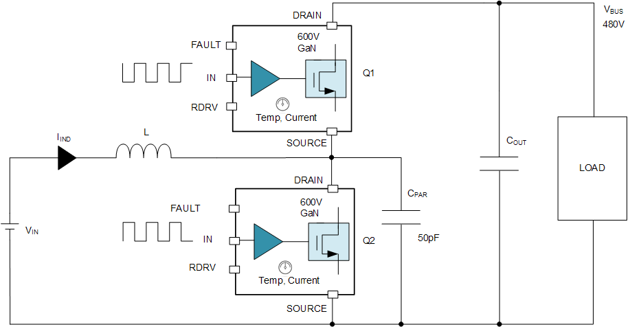
LMG3411R150 LMG3410R150 SOA_Circuit.gifFigure 19. Circuit Used for SOA Curve in Repetitive SOA