SNLS531B April   2016  – June 2018 LMH0324

PRODUCTION DATA.  

  1. Features
  2. Applications
  3. Description
    1.     Device Images
      1.      Simplified Block Diagram
  4. Revision History
  5. Pin Configuration and Functions
    1.     Pin Functions
  6. Specifications
    1. 6.1 Absolute Maximum Ratings
    2. 6.2 ESD Ratings
    3. 6.3 Recommended Operating Conditions
    4. 6.4 Thermal Information
    5. 6.5 Electrical Characteristics
    6. 6.6 Recommended SMBus Interface AC Timing Specifications
    7. 6.7 Serial Parallel Interface (SPI) AC Timing Specifications
    8. 6.8 Typical Characteristics
  7. Detailed Description
    1. 7.1 Overview
    2. 7.2 Functional Block Diagram
    3. 7.3 Feature Description
      1. 7.3.1 4-Level Input Configuration Pins
      2. 7.3.2 Carrier Detect
      3. 7.3.3 Adaptive Cable Equalizer
      4. 7.3.4 Launch Amplitude
      5. 7.3.5 Input-Output Mux Selection
      6. 7.3.6 Output Function Control
      7. 7.3.7 Output Driver Amplitude and De-Emphasis Control
      8. 7.3.8 Additional Programmability
        1. 7.3.8.1 Cable Length Indicator (CLI)
        2. 7.3.8.2 Digital MUTEREF
    4. 7.4 Device Functional Modes
      1. 7.4.1 System Management Bus (SMBus) Mode
        1. 7.4.1.1 SMBus Read and Write Transactions
          1. 7.4.1.1.1 SMBus Write Operation Format
          2. 7.4.1.1.2 SMBus Read Operation Format
      2. 7.4.2 Serial Peripheral Interface (SPI) Mode
        1. 7.4.2.1 SPI Read and Write Transactions
          1. 7.4.2.1.1 SPI Write Transaction Format
          2. 7.4.2.1.2 SPI Read Transaction Format
        2. 7.4.2.2 SPI Daisy Chain
    5. 7.5 LMH0324 Register Map
      1. 7.5.1 Share Register Page
      2. 7.5.2 CableEQ/Drivers Register Page
  8. Application and Implementation
    1. 8.1 Application Information
      1. 8.1.1 General Guidance for SMPTE Applications
    2. 8.2 Typical Application
      1. 8.2.1 Design Requirements
      2. 8.2.2 Detailed Design Procedure
      3. 8.2.3 Recommended VOD and DE Register Settings
      4. 8.2.4 Application Performance Plots
  9. Power Supply Recommendations
  10. 10Layout
    1. 10.1 Layout Guidelines
    2. 10.2 Layout Example
  11. 11Device and Documentation Support
    1. 11.1 Receiving Notification of Documentation Updates
    2. 11.2 Community Resources
    3. 11.3 Trademarks
    4. 11.4 Electrostatic Discharge Caution
    5. 11.5 Glossary
  12. 12Mechanical, Packaging, and Orderable Information

Package Options

Refer to the PDF data sheet for device specific package drawings

Mechanical Data (Package|Pins)
  • RTW|24
Thermal pad, mechanical data (Package|Pins)
Orderable Information

SMBus Read and Write Transactions

SMBus is a two-wire serial interface through which various system component chips can communicate with the master. Slave devices are identified by having a unique device address. The two-wire serial interface consists of SCL and SDA signals. SCL is a clock output from the master to all of the slave devices on the bus. SDA is a bidirectional data signal between the master and slave devices. The LMH0324 SMBus SCL and SDA signals are open drain and require external pull-up resistors.

Start and Stop:

The master generates start and stop patterns at the beginning and end of each transaction.

  • Start: High to low transition (falling edge) of SDA while SCL is high.
  • Stop: Low to high transition (rising edge) of SDA while SCL is high.
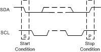
LMH0324 start_stop_conditions_snls515.gifFigure 9. Start and Stop Conditions

The master generates nine clock pulses for each byte transfer. The 9th clock pulse constitutes the ACK cycle. The transmitter releases SDA to allow the receiver to send the ACK signal. An ACK is recorded when the device pulls SDA low, while a NACK is recorded if the line remains high.
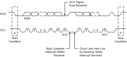
LMH0324 acknowledge_ack_snls515.gifFigure 10. Acknowledge (ACK)