SNLS308G April 2009 – June 2015 LMH0384
PRODUCTION DATA.
- 1 Features
- 2 Applications
- 3 Description
- 4 Revision History
- 5 Pin Configuration and Functions
- 6 Specifications
- 7 Detailed Description
- 8 Application and Implementation
- 9 Power Supply Recommendations
- 10Layout
- 11Device and Documentation Support
- 12Mechanical, Packaging, and Orderable Information
Package Options
Mechanical Data (Package|Pins)
- RUM|16
Thermal pad, mechanical data (Package|Pins)
- RUM|16
Orderable Information
1 Features
- Compliant With ST 424, ST 292, ST 344, and ST 259(1)
- Supports DVB-ASI at 270 Mbps
- Wide Range of Data Rates: 125 Mbps to 2.97 Gbps
- Equalizes up to 140 Meters of Belden 1694A at 2.97 Gbps, up to 200 Meters of Belden 1694A at 1.485 Gbps, or Up to 400 Meters of Belden 1694A at 270 Mbps
- Power Save Mode With Auto Sleep Control (35 mW Typical Power Consumption in Power Save Mode)
- Optional SPI Register Access
- Manual Bypass and Output Mute With a Programmable Threshold
- Internally Terminated 100-Ω LVDS Outputs With SPI Programmable Output Common-Mode Voltage and Swing
- Programmable Launch Amplitude Optimization in SPI Mode
- Cable Length Indicator in SPI Mode
- Single 3.3-V Supply Operation
- 16-Pin WQFN Package
- Industrial Temperature Range: −40°C to +85°C
- Footprint Compatible With the LMH0344, LMH0044, and LMH0074 in Pin Mode
2 Applications
- ST 424, ST 292, ST 344, and ST 259 Serial Digital Interfaces(1)
- Serial Digital Data Equalization and Reception
- Data Recovery Equalization (1)
3 Description
The LMH0384 3-Gbps HD - SD SDI Extended Reach and Configurable Adaptive Cable Equalizer is designed to equalize data transmitted over cable (or any media with similar dispersive loss characteristics). The equalizer operates over a wide range of data rates from 125 Mbps to 2.97 Gbps and supports ST 424, ST 292, ST 344, and ST 259 standards.
The LMH0384 device includes active sensing features and design enhancements including longer cable equalization, lower output jitter, configurable pin mode and SPI modes, a power-saving sleep mode, and programmable output common-mode voltage and swing. The LMH0384 implements DC restoration to correctly handle pathological data conditions.
The LMH0384 includes an auto sleep mode to power down the device when no input signal is detected. Other features include separate carrier detect and output mute pins which may be tied together to mute the output when no input signal is present, and a programmable mute reference which may be used to mute the output at a selectable level of signal degradation.
The LMH0384 supports two modes of operation. In pin mode (non-SPI mode) the LMH0384 is footprint compatible with the LMH0344 and legacy SDI equalizers. In the optional SPI mode, the LMH0384 provides register access to all of its features along with a cable length indicator, programmable output common-mode voltage and swing, and launch amplitude optimization.
Device Information(1)
| PART NUMBER | PACKAGE | BODY SIZE (NOM) |
|---|---|---|
| LMH0384 | WQFN (16) | 4.00 mm × 4.00 mm |
- For all available packages, see the orderable addendum at the end of the data sheet.
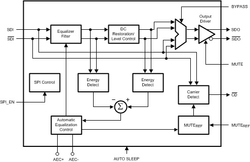
Functional Block Diagram

4 Revision History
Changes from F Revision (April 2013) to G Revision
- Added, updated, or renamed the following sections: Device Information Table, Pin Configuration and Functions; Specifications; Applications and Implementation; Detailed Description; Layout;Device and Documentation Support; Mechanical, Packaging, and Ordering InformationGo
- Added "(logic zero)" to Pin 14 - MUTE - in Pin Descriptions – Pin Mode (non-SPI) / SPI_EN = GND / LMH0344 Compatible table.Go
- Added note "Typical pullup or pulldown for digital pin is 100 kΩ. The tolerance is between 69K to 131K" to DC Electrical CharacteristicsGo
Changes from E Revision (April 2013) to F Revision
- Changed layout of National Data Sheet to TI formatGo