SNWS022D January 2010 – June 2015 LMH2110
PRODUCTION DATA.
- 1 Features
- 2 Applications
- 3 Description
- 4 Revision History
- 5 Pin Configuration and Functions
- 6 Specifications
- 7 Detailed Description
-
8 Application and Implementation
- 8.1 Application Information
- 8.2 Typical Applications
- 9 Power Supply Recommendations
- 10Layout
- 11Device and Documentation Support
- 12Mechanical, Packaging, and Orderable Information
Package Options
Mechanical Data (Package|Pins)
- YFQ|6
Thermal pad, mechanical data (Package|Pins)
Orderable Information
8 Application and Implementation
NOTE
Information in the following applications sections is not part of the TI component specification, and TI does not warrant its accuracy or completeness. TI’s customers are responsible for determining suitability of components for their purposes. Customers must validate and test their design implementation to confirm system functionality.
8.1 Application Information
The LMH2110 is a 45-dB Logarithmic RMS power detector particularly suited for accurate power measurements of modulated RF signals that exhibit large peak-to-average ratios (PARs). The RMS detector implements the exact definition of power resulting in a power measurement insensitive to high PARs. Such signals are encountered, for exampe, in LTE and W-CDMA applications. The LMH2110 has an RF frequency range from
50 MHz to 8 GHz. It provides an output voltage that relates linearly to the RF input power in dBm. Its output voltage is highly insensitive to temperature and supply variations.
8.2 Typical Applications
8.2.1 Application With Transmit Power Control
The LMH2110 can be used in a wide variety of applications such as LTE, W-CDMA, CDMA, and GSM. Transmit-power-control-loop circuits make the transmit power level insensitive to PA inaccuracy. This is desirable because power amplifiers are non-linear devices and temperature dependent, making it hard to estimate the exact transmit power level. If a control loop is used, the inaccuracy of the PA is eliminated from the overall accuracy of the transmit power level. The accuracy of the transmit power level now depends on the RF detector accuracy instead. The LMH2110 is especially suited for transmit power control applications, because it accurately measures transmit power and is insensitive to temperature, supply voltage and modulation variations.
Figure 44 shows a simplified schematic of a typical transmit power control system. The output power of the PA is measured by the LMH2110 through a directional coupler. The measured output voltage of the LMH2110 is digitized by the ADC inside the baseband chip. Accordingly, the baseband controls the PA output power level by changing the gain control signal of the RF VGA. Although the output ripple of the LMH2110 is typically low enough, an optional low-pass filter can be placed in between the LMH2110 and the ADC to further reduce the ripple.
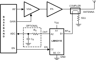 Figure 44. Transmit Power Control System
8.2.1.1 Design Requirements
Some of the design requirements for this logarithmic RMS power detector include:
Table 1. Design Parameters
| DESIGN PARAMETER | EXAMPLE VALUE | |||
|---|---|---|---|---|
| Supply voltage | 2.7 V | |||
| RF input frequency (unmodulated continuous wave) | 1900 MHz | |||
| Minimum power level | –36 dBm | |||
| Maximum power level | 0 dBm | |||
| Maximum output voltage | 1.5 V | |||
8.2.1.2 Detailed Design Procedure
8.2.1.2.1 Specifying Detector Performance
The performance of the LMH2110 can be expressed by a variety of parameters.
8.2.1.2.1.1 Dynamic Range
The LMH2110 is designed to have a predictable and accurate response over a certain input power range. This is called the dynamic range (DR) of a detector. For determining the dynamic range a couple of different criteria can be used. The most commonly used ones are:
- Log conformance error, ELC
- Variation over temperature error, EVOT
- 1-dB step error, E1 dB
- 10-dB step error, E10 dB
- Variation due to modulation, EMOD
The specified dynamic range is the range in which the specified error metric is within a predefined window. See Log Conformance Error, Variation Over Temperature Error, Variation Over Temperature Error, 1-dB Step Error, 10-dB Step Error, and Variation Due to Modulation for an explanation of these errors.
8.2.1.2.1.2 Log Conformance Error
The LMH2110 implements a logarithmic function. In order to describe how close the transfer is to an ideal logarithmic function the log conformance error is used. To calculate the log conformance error the detector transfer function is modeled as a linear-in-dB relationship between the input power and the output voltage.
The ideal linear-in-dB transfer is modeled by 2 parameters:
- Slope
- Intercept
and is described by Equation 9:
where
- KSLOPE is the slope of the line in mV/dB
- PIN the input power level
- PINT is the power level in dBm at which the line intercepts VOUT = 0 V (see Figure 45).
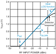 Figure 45. Ideal Logarithmic Response
To determine the log conformance error two steps are required:
- Determine the best fitted line at 25°C.
- Determine the difference between the actual data and the best fitted line.
The best fit can be determined by standard routines. A careful selection of the fit range is important. The fit range must be within the normal range of operation of the device. Outcome of the fit is KSLOPE and PINT.
Subsequently, the difference between the actual data and the best fitted line is determined. The log conformance is specified as an input referred error. The output referred error is therefore divided by the KSLOPE to obtain the input referred error. The log conformance error is calculated by Equation 10:

where
- VOUT is the measured output voltage at a power level at PIN at a temperature. KSLOPE 25°C (mV/dB).
- PINT 25°C (dBm) are the parameters of the best fitted line of the 25°C transfer.
In Figure 46 both the error with respect to the ideal LOG response as well as the error due to temperature variation are included in this error metric. This is because the measured data for all temperatures is compared to the fitted line at 25°C. The measurement result of a typical LMH2110 in Figure 46 shows a dynamic range of
36 dB for ELC = ±1 dB.
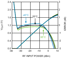 Figure 46. VOUT and ELC vs. RF input Power at 1900 MHz
8.2.1.2.1.3 Variation Over Temperature Error
In contrast to the log conformance error, the variation over temperature error (EVOT) purely measures the error due to temperature variation. The measured output voltage at 25°C is subtracted from the output voltage at another temperature. Subsequently, it is translated into an input referred error by dividing it by KSLOPE at 25°C. Variation over temperature is given by Equation 11:
The variation over temperature is shown in Figure 47, where a dynamic range of 41 dB is obtained
(from PMIN = –36 dBm) for EVOT = ±0.5 dB.
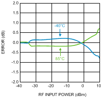 Figure 47. EVOT vs. RF Input Power at 1900 MHz
8.2.1.2.1.4 1-dB Step Error
This parameter is a measure for the error for a 1-dB power step. According to a 3GPP specification, the error must be less than ±0.3 dB. Often, this condition is used to define a useful dynamic range of the detector.
The 1-dB step error is calculated in 3 steps:
- Determine the maximum sensitivity.
- Determine average sensitivity.
- Calculate the 1-dB step error.
First the maximum sensitivity (SMAX) is calculated per temperature by determining the maximum difference between two output voltages for a 1-dB step within the power range:
To calculate the 1-dB step error an average sensitivity (SAVG) is used which is the average of the maximum sensitivity and an allowed minimum sensitivity (SMIN). The allowed minimum sensitivity is determined by the application. In this datasheet SMIN = 30 mV/dB is used. Subsequently, the average sensitivity can be calculated by:
The 1-dB error is than calculated by:
where
- SACTUAL (actual sensitivity) is the difference between two output voltages for a 1-dB step at a given power level.
Figure 48 shows the typical 1-dB step error at 1900 MHz, where a dynamic range of 38 dB over temperature is obtained for E1dB = ±0.3 dB.
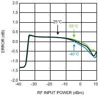 Figure 48. 1-dB Step Error vs. RF Input Power at 1900 MHz
8.2.1.2.1.5 10-dB Step Error
This error is defined in a different manner than the 1-dB step error. This parameter shows the input power error over temperature when a 10-dB power step is made. The 10-dB step at 25°C is taken as a reference.
To determine the 10-dB step error, first the output voltage levels (V1 and V2) for power levels P and P+10 dB” at the 25°C are determined (Figure 49). Subsequently these 2 output voltages are used to determine the corresponding power levels at temperature T (PT and PT + X). The difference between those two power levels minus 10 results in the 10-dB step error.
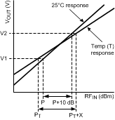 Figure 49. Graphical Representation of 10-dB Step Calculations
Figure 50 shows the typical 10-dB step error at 1900 MHz, where a dynamic range of 30 dB is obtained for
E10dB = ±1 dB.
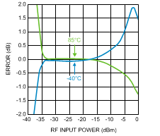 Figure 50. 10 dB Step Error vs. RF Input Power at 1900 MHz
8.2.1.2.1.6 Variation Due to Modulation
The response of an RF detector may vary due to different modulation schemes. How much it varies depends on the modulation form and the type of detector. Modulation forms with high peak-to-average ratios (PAR) can cause significant variation, especially with traditional RF detectors. This is because the measurement is not an actual RMS measurement and is therefore waveform dependent.
To calculate the variation due to modulation (EMOD), the measurement result for an un-modulated RF carrier is subtracted from the measurement result of a modulated RF carrier. The calculations are similar to those for variation over temperature. The variation due to modulation can be calculated by:
where
- VOUT_MOD is the measured output voltage for an applied power level of a modulated signal.
- VOUT_CW is the output voltage as a result of an applied un-modulated signal having the same power level.
Figure 51 shows the variation due to modulation for W-CDMA, where a EMOD of 0.09 dB in obtained for a dynamic range from –38 dBm to –5 dBm.
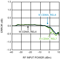 Figure 51. Variation Due to Modulation for W-CDMA
8.2.1.3 Application Curves
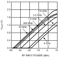 Figure 52. Output Voltage vs. RF Input Power
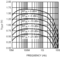 Figure 53. Output Voltage vs. Frequency
8.2.2 Application With Resistive Divider
RF systems typically use a characteristic impedance of 50 Ω. The LMH2110 is no exception to this. The RF input pin of the LMH2110 has an input impedance of 50 Ω. It enables an easy, direct connection to a directional coupler without the need for additional components (Figure 44). For an accurate power measurement the input power range of the LMH2110 needs to be aligned with the output power range of the power amplifier. This can be done by selecting a directional coupler with the correct coupling factor.
Because the LMH2110 has a constant input impedance, a resistive divider can also be used instead of a directional coupler (Figure 54).
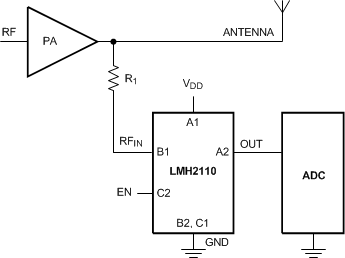 Figure 54. Application With Resistive Divider
Resistor R1 implements an attenuator together with the detector input impedance to match the output range of the PA to the input range of the LMH2110. The attenuation (AdB) realized by R1 and the effective input impedance of the LMH2110 equals:

Solving Equation 16 for R1 yields:

Suppose the desired attenuation is 30 dB with a given LMH2110 input impedance of 50 Ω, the resistor R1 needs to be 1531 Ω. A practical value is 1.5 kΩ. Although this is a cheaper solution than the application with directional coupler, it also comes with a disadvantage. After calculating the resistor value it is possible that the realized attenuation is less then expected. This is because of the parasitic capacitance of resistor R1 which results in a lower actual realized attenuation. Whether the attenuation is reduced depends on the frequency of the RF signal and the parasitic capacitance of resistor R1. Because the parasitic capacitance varies from resistor to resistor, exact determination of the realized attenuation can be difficult. A way to reduce the parasitic capacitance of resistor R1 is to realize it as a series connection of several separate resistors.
8.2.3 Application With Low-Pass Output Filter for Residual Ripple Reduction
The output of the LMH2110 provides a DC voltage that is a measure for the applied RF power to the input pin. The output voltage has a linear-in-dB response for an applied RF signal.
RF power detectors can have some residual ripple on the output due to the modulation of the applied RF signal. The residual ripple on the output of the LMH2110 device is small though and, therefore, additional filtering is usually not needed. This is because its internal averaging mechanism reduces the ripple significantly. For some modulation types however, having very high peak-to-average ratios, additional filtering might be useful.
Filtering can be applied by an external low-pass filter. Filtering reduces not only the ripple, but also increases the response time. In other words, it takes longer before the output reaches its final value. A trade-off must be made between allowed ripple and allowed response time. The filtering technique is depicted in Figure 55. The filtering of the low pass output filter is realized by resistor RS and capacitor CS. The –3-dB bandwidth of this filter can be calculated by:
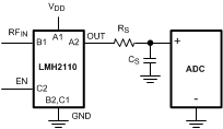 Figure 55. Low-Pass Output Filter for Residual Ripple Reduction
The output impedance of the LMH2110 is HIGH in shutdown. This is especially beneficial in pulsed mode systems. It ensures a fast settling time when the device returns from shutdown into active mode and reduces power consumption.
In pulse mode systems, the device is active only during a fraction of the time. During the remaining time the device is in low-power shutdown. Pulsed mode system applications usually require that the output value is available at all times. This can be realized by a capacitor connected between the output and GND that “stores” the output voltage level. To apply this principle, capacitor discharging must be minimized in shutdown mode. The connected ADC input must therefore have a high input impedance to prevent a possible discharge path through the ADC. When an additional filter is applied at the output, the capacitor of the RC-filter can be used to store the output value. An LMH2110 with a high impedance shutdown mode saves power in pulse mode systems. This is because the capacitor CS does not need to be fully re-charged each cycle.