SBOS709A July   2016  – July 2016 LMH2832

PRODUCTION DATA.  

  1. Features
  2. Applications
  3. Description
  4. Revision History
  5. Device Comparison Table
  6. Pin Configuration and Functions
  7. Specifications
    1. 7.1 Absolute Maximum Ratings
    2. 7.2 ESD Ratings
    3. 7.3 Recommended Operating Conditions
    4. 7.4 Thermal Information
    5. 7.5 Electrical Characteristics
    6. 7.6 Timing Requirements: SPI
    7. 7.7 Typical Characteristics
  8. Parameter Measurement Information
    1. 8.1 Setup Diagrams
    2. 8.2 ATE Testing and DC Measurements
    3. 8.3 Frequency Response
    4. 8.4 Distortion
    5. 8.5 Noise Figure
    6. 8.6 Pulse Response, Slew Rate, and Overdrive Recovery
    7. 8.7 Power-Down
    8. 8.8 Crosstalk, Gain Matching, and Phase Matching
    9. 8.9 Output Measurement Reference Points
  9. Detailed Description
    1. 9.1 Overview
    2. 9.2 Functional Block Diagram
    3. 9.3 Feature Description
      1. 9.3.1 Analog Input Characteristics
      2. 9.3.2 Analog Output Characteristics
      3. 9.3.3 Driving Low Insertion-Loss Filters
      4. 9.3.4 Input Impedance Matching
      5. 9.3.5 Power-On Reset (POR)
    4. 9.4 Device Functional Modes
      1. 9.4.1 Power-Down (PD)
      2. 9.4.2 Gain Control
    5. 9.5 Programming
      1. 9.5.1 Details of the Serial Interface
      2. 9.5.2 Timing Diagrams
    6. 9.6 Register Maps
      1. 9.6.1 Register Descriptions
        1. 9.6.1.1 SW Reset Register (address = 2)
      2. 9.6.2 Power-Down Control Register (address = 3)
      3. 9.6.3 Channel A RW0 Register (address = 4)
      4. 9.6.4 Channel A RW1 Register (address = 5)
      5. 9.6.5 Channel B RW0 Register (address = 6)
      6. 9.6.6 Channel B RW1 Register (address = 7)
  10. 10Application and Implementation
    1. 10.1 Application Information
      1. 10.1.1 Driving ADCs
        1. 10.1.1.1 SNR Considerations
        2. 10.1.1.2 SFDR Considerations
        3. 10.1.1.3 ADC Input Common-Mode Voltage Considerations (AC-Coupled Input)
        4. 10.1.1.4 ADC Input Common-Mode Voltage Considerations (DC-Coupled Input)
    2. 10.2 Typical Applications
      1. 10.2.1 DOCSIS 3.X Driver
        1. 10.2.1.1 Design Requirements
        2. 10.2.1.2 Detailed Design Procedure
          1. 10.2.1.2.1 Source Resistance Matching
          2. 10.2.1.2.2 Output Impedance Matching
          3. 10.2.1.2.3 Voltage Headroom Considerations
        3. 10.2.1.3 Application Curve
      2. 10.2.2 IQ Receiver
    3. 10.3 Do's and Don'ts
      1. 10.3.1 Do:
      2. 10.3.2 Don't:
  11. 11Power Supply Recommendations
    1. 11.1 Split Supplies
    2. 11.2 Supply Decoupling
  12. 12Layout
    1. 12.1 Layout Guidelines
    2. 12.2 Layout Example
  13. 13Device and Documentation Support
    1. 13.1 Device Support
      1. 13.1.1 Device Nomenclature
    2. 13.2 Documentation Support
      1. 13.2.1 Related Documentation
    3. 13.3 Receiving Notification of Documentation Updates
    4. 13.4 Community Resources
    5. 13.5 Trademarks
    6. 13.6 Electrostatic Discharge Caution
    7. 13.7 Glossary
  14. 14Mechanical, Packaging, and Orderable Information

Package Options

Mechanical Data (Package|Pins)
Thermal pad, mechanical data (Package|Pins)
Orderable Information

12 Layout

12.1 Layout Guidelines

With a small bandwidth greater than 1 GHz, layout for the LMH2832 is critical and nothing can be neglected. In order to simplify board design, the LMH2832 has on-chip resistors that reduce the affect of off-chip capacitance. For this reason, make sure that the ground layer below the LMH2832 is not cut. The recommendation to not cut the ground plane under the amplifier input and output pins is different than many other high-speed amplifiers, but the reason is that parasitic inductance is more harmful to the LMH2832 performance than parasitic capacitance. By leaving the ground layer under the device intact, parasitic inductance of the output and power traces is minimized. The DUT portion of the evaluation board layout is shown in Figure 63.

The EVM uses long-edge capacitors for the decoupling capacitors, which reduces series resistance and increases the resonant frequency. Vias are also placed to the power planes before the bypass capacitors. Although not evident in the top layer, two vias are used at the capacitor in addition to the two vias underneath the device.

The output-matching resistors are 0402 size and are placed very close to the amplifier output pins, which reduces both parasitic inductance and capacitance. The use of 0603 output-matching resistors produces a measurable decrease in bandwidth.

When the signal is on a 50-Ω or 75-Ω controlled impedance transmission line, the layout then becomes much less critical. The transition from the 50-Ω or 75-Ω transmission line to the amplifier pins is the most critical area.

12.2 Layout Example
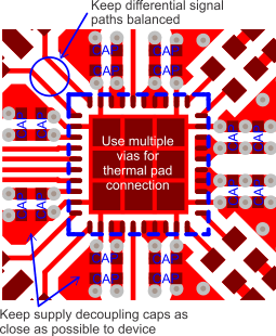
LMH2832 layout_sbos709.gif Figure 63. Layout Example