SBOS965D October 2019 – January 2023 LMH32401
PRODUCTION DATA
- 1 Features
- 2 Applications
- 3 Description
- 4 Revision History
- 5 Pin Configuration and Functions
-
6 Specifications
- 6.1 Absolute Maximum Ratings
- 6.2 ESD Ratings
- 6.3 Recommended Operating Conditions
- 6.4 Thermal Information
- 6.5 Electrical Characteristics: Gain = 2 kΩ
- 6.6 Electrical Characteristics: Gain = 20 kΩ
- 6.7 Electrical Characteristics: Both Gains
- 6.8 Electrical Characteristics: Logic Threshold and Switching Characteristics
- 6.9 Typical Characteristics
- 7 Detailed Description
- 8 Application and Implementation
- 9 Power Supply Recommendations
- 10Layout
- 11Device and Documentation Support
- 12Mechanical, Packaging, and Orderable Information
Package Options
Refer to the PDF data sheet for device specific package drawings
Mechanical Data (Package|Pins)
- RGT|16
- Y|0
Thermal pad, mechanical data (Package|Pins)
- RGT|16
Orderable Information
8.1 Application Information
The differential outputs of the LMH32401 device can directly drive a high-speed differential input ADC. Figure 8-1 shows the LMH32401 differential outputs directly driving the ADC12QJ1600. The effective signal gain between the TIA input and the ADC input is 2 kΩ or 20 kΩ when driving an ADC with a 100-Ω differential input impedance (RADC_IN = 50 Ω). Equation 2 gives the effective signal gain between the TIA input and the ADC input when driving an ADC with any other value of differential input impedance (RADC_IN ≠ 50 Ω).
 Figure 8-1 LMH32401 to ADC Interface
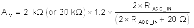
Where:
- AV = Differential gain from the TIA input to the ADC input
- RADC_IN = Input resistance of the ADC
Figure 8-2 shows a matching resistor network between the LMH32401 output and the ADC12QJ1600 input. The matching network is needed to prevent signal reflections when the signal path between the LMH32401 and ADC is very long. Equation 3 gives the effective gain from the TIA input to the ADC input when using a matching resistor network.
 Figure 8-2 LMH32401 to ADC Interface with a Matching Resistor Network
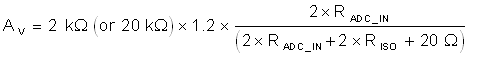
Where:
- AV = Gain from the TIA input to the ADC input
- RADC_IN = Differential input resistance of the ADC
- RISO = Series resistance between the TIA and ADC
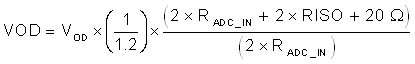
Equation 4 gives the voltage to be applied at the VOD pin (pin 9) if a certain differential offset voltage (VOD) is needed at the ADC input for the circuit in Figure 8-2.
Where:
- VOD = Voltage applied at pin 9
- VOD = Desired differential offset voltage at the ADC input
- RADC_IN = Differential input resistance of the ADC
- RISO = Series resistance between the TIA and ADC