SNAS579G March 2012 – December 2014 LMK00105
PRODUCTION DATA.
- 1 Features
- 2 Applications
- 3 Description
- 4 Revision History
- 5 Pin Configuration and Diagrams
- 6 Specifications
- 7 Detailed Description
- 8 Application and Implementation
- 9 Power Supply Recommendations
- 10Layout
- 11Device and Documentation Support
- 12Mechanical, Packaging, and Orderable Information
Package Options
Refer to the PDF data sheet for device specific package drawings
Mechanical Data (Package|Pins)
- RTW|24
Thermal pad, mechanical data (Package|Pins)
Orderable Information
9.2 Power Supply Ripple Rejection
In practical system applications, power supply noise (ripple) can be generated from switching power supplies, digital ASICs or FPGAs, etc. While power supply bypassing will help filter out some of this noise, it is important to understand the effect of power supply ripple on the device performance. When a single-tone sinusoidal signal is applied to the power supply of a clock distribution device, such as LMK00105, it can produce narrow-band phase modulation as well as amplitude modulation on the clock output (carrier). In the singleside band phase noise spectrum, the ripple-induced phase modulation appears as a phase spur level relative to the carrier (measured in dBc).
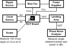
For the LMK00105, power supply ripple rejection (PSRR), was measured as the single-sideband phase spur level (in dBc) modulated onto the clock output when a ripple signal was injected onto the Vddo supply. The PSRR test setup is shown in Figure 22.
 Figure 22. PSRR Test Setup
A signal generator was used to inject a sinusoidal signal onto the Vddo supply of the DUT board, and the peak-to-peak ripple amplitude was measured at the Vddo pins of the device. A limiting amplifier was used to remove amplitude modulation on the differential output clock and convert it to a single-ended signal for the phase noise analyzer. The phase spur level measurements were taken for clock frequencies of 100 MHz under the following power supply ripple conditions:
- Ripple amplitude: 100 mVpp on Vddo = 2.5 V
- Ripple frequency: 100 kHz
Assuming no amplitude modulation effects and small index modulation, the peak-to-peak deterministic jitter (DJ) can be calculated using the measured single-sideband phase spur level (PSRR) as follows: