SNAS636C December   2013  – July 2021 LMK00338

PRODUCTION DATA  

  1. Features
  2. Applications
  3. Description
  4. Revision History
  5. Pin Configuration and Functions
  6. Specifications
    1. 6.1 Absolute Maximum Ratings
    2. 6.2 ESD Ratings
    3. 6.3 Recommended Operating Conditions
    4. 6.4 Thermal Information
    5. 6.5 Electrical Characteristics
    6. 6.6 Typical Characteristics
  7. Parameter Measurement Information
    1. 7.1 Differential Voltage Measurement Terminology
  8. Detailed Description
    1. 8.1 Overview
    2. 8.2 Functional Block Diagram
    3. 8.3 Feature Description
      1. 8.3.1 Crystal Power Dissipation vs. RLIM
      2. 8.3.2 Clock Inputs
      3. 8.3.3 Clock Outputs
        1. 8.3.3.1 Reference Output
    4. 8.4 Device Functional Modes
      1. 8.4.1 VCC and VCCO Power Supplies
  9. Power Supply Recommendations
    1. 9.1 Current Consumption and Power Dissipation Calculations
      1. 9.1.1 Power Dissipation Example: Worst-Case Dissipation
    2. 9.2 Power Supply Bypassing
      1. 9.2.1 Power Supply Ripple Rejection
  10. 10Layout
    1. 10.1 Layout Guidelines
    2. 10.2 Layout Example
    3. 10.3 Thermal Management
  11. 11Device and Documentation Support
    1. 11.1 Documentation Support
      1. 11.1.1 Related Documentation
    2. 11.2 Receiving Notification of Documentation Updates
    3. 11.3 Support Resources
    4. 11.4 Trademarks
    5. 11.5 Electrostatic Discharge Caution
    6. 11.6 Glossary

Package Options

Mechanical Data (Package|Pins)
Thermal pad, mechanical data (Package|Pins)
Orderable Information

Typical Characteristics

Unless otherwise specified: VCC = 3.3 V, VCCO = 3.3 V, TA = 25°C, CLKin driven differentially, input slew rate ≥ 3 V/ns.
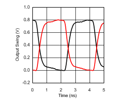
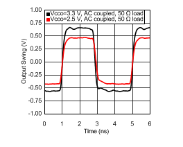
GUID-8EBDCA62-DA58-4F26-B3C9-2DEF8F359D22-low.gifFigure 6-1 HCSL Output Swing at 250 MHz
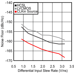
GUID-D1DDED55-8D14-40A4-A10B-4DEA4FEC8CFA-low.gif
Fclk = 100 MHzFoffset = 20 MHz
Figure 6-3 Noise Floor vs CLKin Slew Rate at 100 MHz
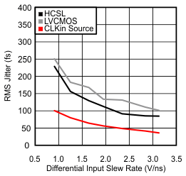
GUID-04B5CA37-C2FC-4346-BBCD-AB680C5C8B2D-low.gif
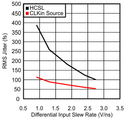
Fclk = 100 MHzInt. BW = 1 to 20 MHz
Figure 6-5 RMS Jitter vs CLKin Slew Rate at 100 MHz
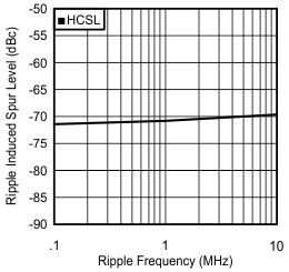
GUID-1E342A6A-8AFB-46D6-B48C-F449D585D72A-low.gif
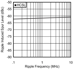
Fclk = 156.25 MHzVCCO Ripple = 100
Figure 6-7 PSRR vs Ripple Frequency at 156.25 MHz
GUID-3E928DA2-7D85-4BA2-A04B-46C202FDA158-low.gifFigure 6-9 Propagation Delay vs Temperature
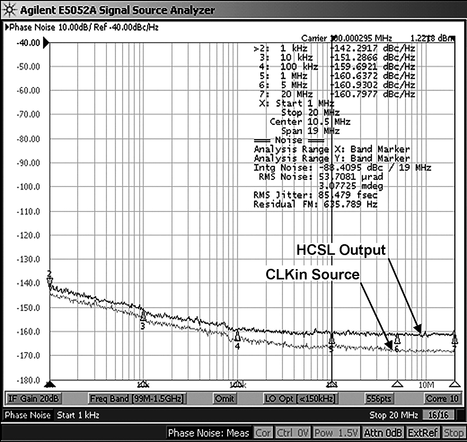
GUID-33C4D9E6-08D8-4B20-99B1-9A605A734B4E-low.pngFigure 6-11 HCSL Phase Noise at 100 MHz
GUID-E577754B-7ECC-42C0-92F8-6C10AD85D788-low.gifFigure 6-2 LVCMOS Output Swing at 250 MHz
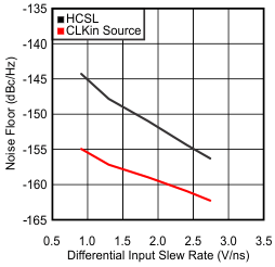
GUID-049778B3-5F9D-4F12-B659-90B0891071DB-low.gif
Fclk = 156.25 MHzFoffset = 20 MHz
Figure 6-4 Noise Floor vs CLKin Slew Rate at 156.25 MHz
GUID-AE26DB55-FD7B-479E-A9EB-0F417B47823F-low.gif
Fclk = 156.25 MHzInt. BW = 1 to 20 MHz
Figure 6-6 RMS Jitter vs CLKin Slew Rate at 156.25 MHz
GUID-C4195F15-E70B-4AE1-9B9A-229DD3FB585F-low.gif
Fclk = 312.5 MHzVCCO Ripple = 100 mVpp
Figure 6-8 PSRR vs Ripple Frequency at 312.5 MHz
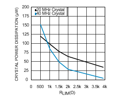
GUID-347942B2-052B-45D9-9640-94A20480E8B3-low.gifFigure 6-10 Crystal Power Dissipation vs RLIM