SNAS791D December 2019 – February 2022 LMK1C1102 , LMK1C1103 , LMK1C1104
PRODUCTION DATA
- 1 Features
- 2 Applications
- 3 Description
- 4 Revision History
- 5 Device Comparison
- 6 Pin Configuration and Functions
- 7 Specifications
- 8 Parameter Measurement Information
- 9 Detailed Description
- 10Application and Implementation
- 11Power Supply Recommendations
- 12Layout
- 13Device and Documentation Support
- 14Mechanical, Packaging, and Orderable Information
Package Options
Mechanical Data (Package|Pins)
Thermal pad, mechanical data (Package|Pins)
Orderable Information
10.2.3 Application Curves
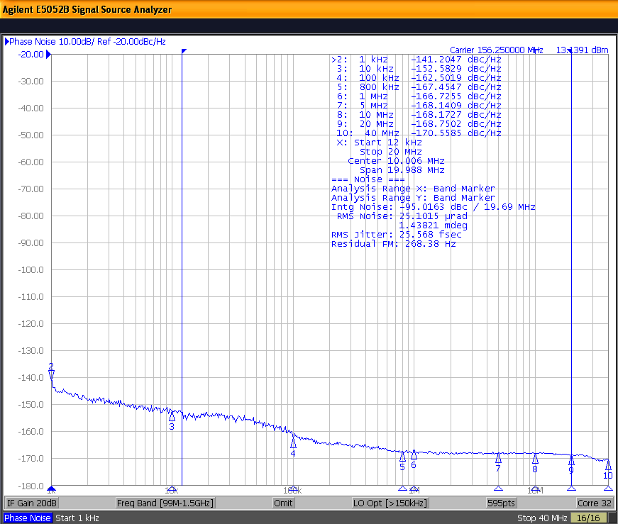
The low additive jitter of the LMK1C110x is shown in Figure 10-2.
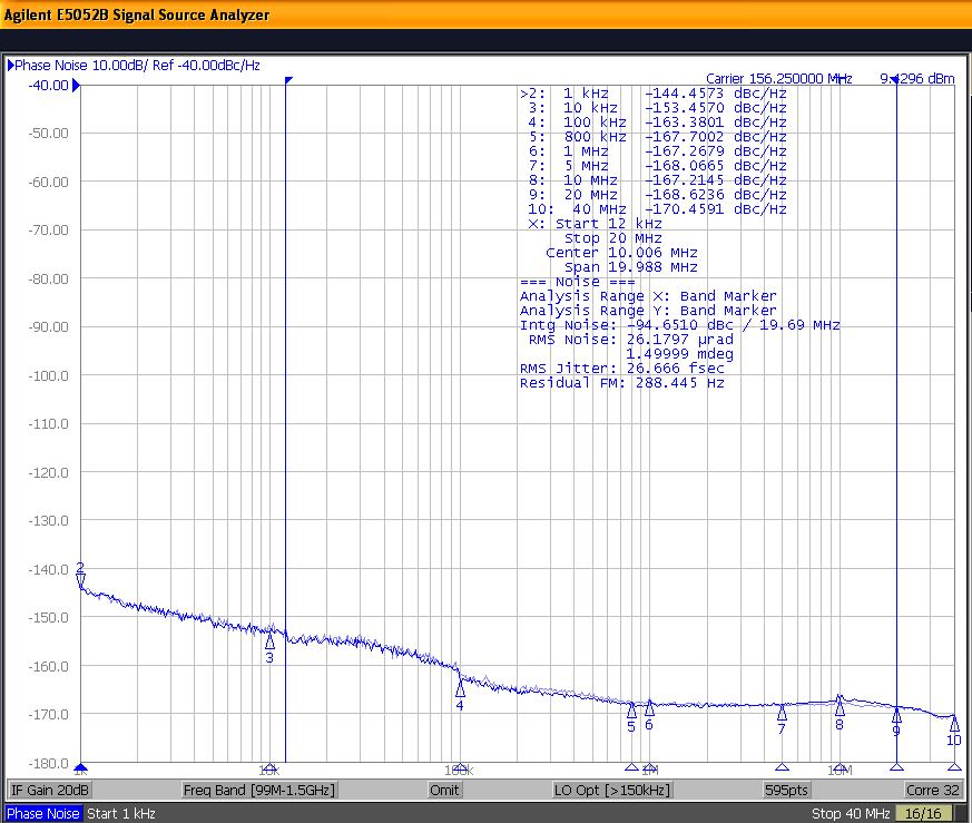
Figure 10-3 shows the low-noise 156.25-MHz reference source with 25.6-fs RMS jitter driving the LMK1C110x, resulting in 26.7-fs RMS jitter when integrated from 12 kHz to 20 MHz at 3.3-V supply. The resultant additive jitter measured is a low 7.6-fs RMS for this configuration.
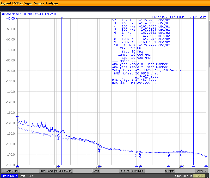
Figure 10-4 shows the low-noise 156.25-MHz reference source with 25.6-fs RMS jitter driving the LMK1C110x, resulting in 27.5-fs RMS jitter when integrated from 12 kHz to 20 MHz at 2.5-V supply. The resultant additive jitter measured is a low 10-fs RMS for this configuration.
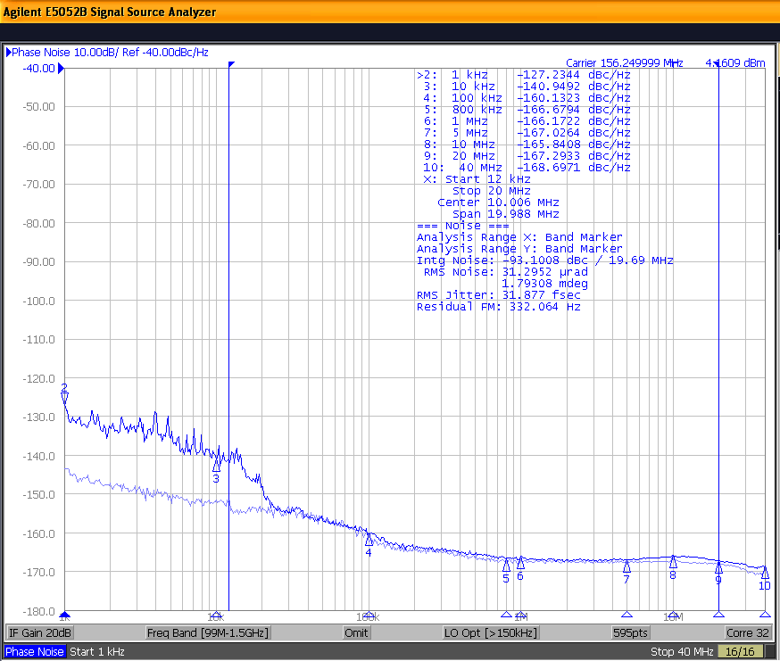
Figure 10-5 shows the low-noise 156.25-MHz reference source with 25.6-fs RMS jitter driving the LMK1C110x, resulting in 32-fs RMS jitter when integrated from 12 kHz to 20 MHz at 1.8-V supply. The resultant additive jitter measured is a low 19.2-fs RMS for this configuration.
 Figure 10-2 LMK1C110x Reference Phase
Noise 25.6-fs (12 kHz to 20 MHz)
 Figure 10-4 LMK1C110x 2.5-V Output
Phase Noise 27.5-fs (12 kHz to 20 MHz)
 Figure 10-3 LMK1C110x 3.3-V Output
Phase Noise 26.7-fs (12 kHz to 20 MHz)
 Figure 10-5 LMK1C110x 1.8-V Output
Phase Noise 32-fs (12 kHz to 20 MHz)