SNAS750B November   2020  – March 2021 LMK5C33216

PRODUCTION DATA  

  1. Features
  2. Applications
  3. Description
  4. Revision History
  5. Device Comparison
  6. Pin Configuration and Functions
  7. Specifications
    1. 7.1 Absolute Maximum Ratings
    2. 7.2 ESD Ratings
    3. 7.3 Recommended Operating Conditions
    4. 7.4 Thermal Information
    5. 7.5 Electrical Characteristics
    6. 7.6 Timing Diagrams
  8. Parameter Measurement Information
    1. 8.1 Differential Voltage Measurement Terminology
    2. 8.2 Output Clock Test Configurations
  9. Detailed Description
    1. 9.1 Overview
    2. 9.2 Functional Block Diagram
      1. 9.2.1 PLL Architecture Overview
      2. 9.2.2 DPLL
        1. 9.2.2.1 Independent DPLL Operation
        2. 9.2.2.2 Cascaded DPLL Operation
        3. 9.2.2.3 APLL Cascaded with DPLL
      3. 9.2.3 APLL-Only Mode
    3. 9.3 Feature Description
      1. 9.3.1  Oscillator Input (XO)
      2. 9.3.2  Reference Inputs
      3. 9.3.3  Clock Input Interfacing and Termination
      4. 9.3.4  Reference Input Mux Selection
        1. 9.3.4.1 Automatic Input Selection
        2. 9.3.4.2 Manual Input Selection
      5. 9.3.5  Hitless Switching
        1. 9.3.5.1 Hitless Switching with Phase Cancellation
        2. 9.3.5.2 Hitless Switching With Phase Slew Control
        3. 9.3.5.3 Hitless Switching With 1-PPS Inputs
      6. 9.3.6  Gapped Clock Support on Reference Inputs
      7. 9.3.7  Input Clock and PLL Monitoring, Status, and Interrupts
        1. 9.3.7.1 XO Input Monitoring
        2. 9.3.7.2 Reference Input Monitoring
          1. 9.3.7.2.1 Reference Validation Timer
          2. 9.3.7.2.2 Frequency Monitoring
          3. 9.3.7.2.3 Missing Pulse Monitor (Late Detect)
          4. 9.3.7.2.4 Runt Pulse Monitor (Early Detect)
          5. 9.3.7.2.5 Phase Valid Monitor for 1-PPS Inputs
        3. 9.3.7.3 PLL Lock Detectors
        4. 9.3.7.4 Tuning Word History
        5. 9.3.7.5 Status Outputs
        6. 9.3.7.6 Interrupt
      8. 9.3.8  PLL Relationships
        1. 9.3.8.1  PLL Frequency Relationships
          1. 9.3.8.1.1 APLL Phase Detector Frequency
          2. 9.3.8.1.2 APLL VCO Frequency
          3. 9.3.8.1.3 DPLL TDC Frequency
          4. 9.3.8.1.4 DPLL VCO Frequency
          5. 9.3.8.1.5 Clock Output Frequency
        2. 9.3.8.2  Analog PLLs (APLL1, APLL2, APLL3)
        3. 9.3.8.3  APLL Reference Paths
          1. 9.3.8.3.1 APLL XO Doubler
          2. 9.3.8.3.2 APLL XO Reference (R) Divider
        4. 9.3.8.4  APLL Phase Frequency Detector (PFD) and Charge Pump
        5. 9.3.8.5  APLL Feedback Divider Paths
          1. 9.3.8.5.1 APLL N Divider with SDM
        6. 9.3.8.6  APLL Loop Filters (LF1, LF2, LF3)
        7. 9.3.8.7  APLL Voltage Controlled Oscillators (VCO1, VCO2, VCO3)
          1. 9.3.8.7.1 VCO Calibration
        8. 9.3.8.8  APLL VCO Clock Distribution Paths
        9. 9.3.8.9  DPLL Reference (R) Divider Paths
        10. 9.3.8.10 DPLL Time-to-Digital Converter (TDC)
        11. 9.3.8.11 DPLL Loop Filter (DLF)
        12. 9.3.8.12 DPLL Feedback (FB) Divider Path
      9. 9.3.9  Output Clock Distribution
      10. 9.3.10 Output Channel Muxes
      11. 9.3.11 Output Dividers (OD)
      12. 9.3.12 SYSREF
      13. 9.3.13 Output Delay
      14. 9.3.14 Clock Outputs (OUTx_P/N)
        1. 9.3.14.1 Differential Output
        2. 9.3.14.2 LVCMOS Output
        3. 9.3.14.3 Output Auto-Mute During LOL
      15. 9.3.15 Glitchless Output Clock Start-Up
      16. 9.3.16 Clock Output Interfacing and Termination
      17. 9.3.17 Output Synchronization (SYNC)
      18. 9.3.18 Zero-Delay Mode (ZDM) Synchronization
      19. 9.3.19 Time of Day (ToD) Counter
        1. 9.3.19.1 Configuring ToD Functionality
        2. 9.3.19.2 SPI as a Trigger Source
        3. 9.3.19.3 GPIO Pin as a ToD Trigger Source
          1. 9.3.19.3.1 An Example: Making a time measurement using ToD and GPIO1 as trigger
        4. 9.3.19.4 ToD Timing
        5. 9.3.19.5 Other ToD Behavior
    4. 9.4 Device Functional Modes
      1. 9.4.1 Device Start-Up
        1. 9.4.1.1 ROM Selection
        2. 9.4.1.2 EEPROM Overlay
      2. 9.4.2 DPLL Operating States
        1. 9.4.2.1 Free-Run
        2. 9.4.2.2 Lock Acquisition
        3. 9.4.2.3 DPLL Locked
        4. 9.4.2.4 Holdover
      3. 9.4.3 PLL Start-Up Sequence
      4. 9.4.4 Digitally-Controlled Oscillator (DCO) Frequency and Phase Adjustment
        1. 9.4.4.1 DPLL DCO Control
          1. 9.4.4.1.1 DPLL DCO Relative Adjustment Frequency Step Size
          2. 9.4.4.1.2 APLL DCO Frequency Step Size
      5. 9.4.5 APLL Frequency Control
      6. 9.4.6 Zero-Delay Mode Synchronization
    5. 9.5 Programming
      1. 9.5.1 Interface and Control
      2. 9.5.2 I2C Serial Interface
        1. 9.5.2.1 I2C Block Register Transfers
      3. 9.5.3 SPI Serial Interface
        1. 9.5.3.1 SPI Block Register Transfer
      4. 9.5.4 Register Map Generation
      5. 9.5.5 General Register Programming Sequence
  10. 10Application and Implementation
    1. 10.1 Application Information
      1. 10.1.1 Device Start-Up Sequence
      2. 10.1.2 Power Down (PD#) Pin
      3. 10.1.3 Strap Pins for Start-Up
      4. 10.1.4 ROM and EEPROM
      5. 10.1.5 Power Rail Sequencing, Power Supply Ramp Rate, and Mixing Supply Domains
        1. 10.1.5.1 Power-On Reset (POR) Circuit
        2. 10.1.5.2 Powering Up From a Single-Supply Rail
        3. 10.1.5.3 Power Up From Split-Supply Rails
        4. 10.1.5.4 Non-Monotonic or Slow Power-Up Supply Ramp
      6. 10.1.6 Slow or Delayed XO Start-Up
    2. 10.2 Typical Application
      1. 10.2.1 Design Requirements
      2. 10.2.2 Detailed Design Procedure
    3. 10.3 Do's and Don'ts
  11. 11Power Supply Recommendations
    1. 11.1 Power Supply Bypassing
  12. 12Layout
    1. 12.1 Layout Guidelines
    2. 12.2 Layout Example
    3. 12.3 Thermal Reliability
      1. 12.3.1 Support for PCB Temperature up to 105°C
  13. 13Device and Documentation Support
    1. 13.1 Documentation Support
      1. 13.1.1 Related Documentation
    2. 13.2 Receiving Notification of Documentation Updates
    3. 13.3 Support Resources
    4. 13.4 Trademarks
    5. 13.5 Glossary
    6. 13.6 Electrostatic Discharge Caution
  14. 14Mechanical, Packaging, and Orderable Information

Package Options

Mechanical Data (Package|Pins)
Thermal pad, mechanical data (Package|Pins)
Orderable Information

Differential Voltage Measurement Terminology

The differential voltage of a differential signal can be described by two different definitions, causing confusion when reading data sheets or communicating with other engineers. This section will address the measurement and description of a differential signal so that the reader is able to understand and distinguish between the two different definitions when used.

The first definition used to describe a differential signal is the absolute value of the voltage potential between the inverting and noninverting signal. The symbol for this first measurement is typically VID or VOD depending on if an input or output voltage is being described.

The second definition used to describe a differential signal is to measure the potential of the noninverting signal with respect to the inverting signal. The symbol for this second measurement is VSS and is a calculated parameter. Nowhere in the IC does this signal exist with respect to ground, it only exists in reference to its differential pair. VSS can be measured directly by oscilloscopes with floating references, otherwise this value can be calculated as twice the value of VOD as described in the first description.

Figure 8-1 illustrates the two different definitions side-by-side for inputs and Figure 8-2 illustrates the two different definitions side-by-side for outputs. The VID and VOD definitions show VA and VB DC levels that the noninverting and inverting signals toggle between with respect to ground. VSS input and output definitions show that if the inverting signal is considered the voltage potential reference, the noninverting signal voltage potential is now increasing and decreasing above and below the noninverting reference. Thus the peak-to-peak voltage of the differential signal can be measured.

VID and VOD are often defined as volts (V) and VSS is often defined as volts peak-to-peak (VPP).
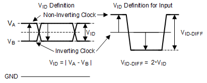
GUID-20201023-CA0I-8QDQ-P0BS-HLP3NJK2F17G-low.gif Figure 8-1 Two Different Definitions for Differential Input Signals
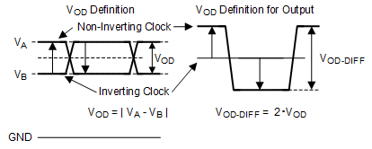
GUID-20201023-CA0I-HQSK-B0JD-QC4CTBZDV8PD-low.gif Figure 8-2 Two Different Definitions for Differential Output Signals