SNAS675A October 2015 – November 2015 LMK61PD0A2
PRODUCTION DATA.
- 1 Features
- 2 Applications
- 3 Description
- 4 Revision History
- 5 Device Control
- 6 Pin Configuration and Functions
-
7 Specifications
- 7.1 Absolute Maximum Ratings
- 7.2 ESD Ratings
- 7.3 Recommended Operating Conditions
- 7.4 Thermal Information
- 7.5 Electrical Characteristics - Power Supply
- 7.6 LVPECL Output Characteristics
- 7.7 LVDS Output Characteristics
- 7.8 HCSL Output Characteristics
- 7.9 OE Input Characteristics
- 7.10 OS, FS[1:0] Input Characteristics
- 7.11 Frequency Tolerance Characteristics
- 7.12 Power-On/Reset Characteristics (VDD)
- 7.13 PSRR Characteristics
- 7.14 PLL Clock Output Jitter Characteristics
- 7.15 Additional Reliability and Qualification
- 7.16 Typical Performance Characteristics
- 8 Parameter Measurement Information
- 9 Detailed Description
- 10Application and Implementation
- 11Power Supply Recommendations
- 12Layout
- 13Device and Documentation Support
- 14Mechanical, Packaging, and Orderable Information
Package Options
Mechanical Data (Package|Pins)
- SIA|8
Thermal pad, mechanical data (Package|Pins)
Orderable Information
1 Features
-
Ultra-low Noise, High Performance
- Jitter: 90 fs RMS typical fOUT > 100 MHz
- PSRR: -70 dBc, robust supply noise immunity
- Flexible Output Frequency and Format; User Selectable
- Frequencies: 62.5 MHz, 100 MHz, 106.25 MHz, 125 MHz, 156.25 MHz, 212.5 MHz, 312.5 MHz
- Formats: LVPECL, LVDS or HCSL
- Total frequency tolerance of ± 50 ppm
- Internal memory stores multiple start-up configurations, selectable through pin control
- 3.3V operating voltage
- Industrial temperature range (-40ºC to +85ºC)
- 7 mm x 5 mm 8-pin package
2 Applications
- High-performance replacement for crystal-, SAW-, or silicon-based Oscillators
- Switches, Routers, Network Line Cards, Base Band Units (BBU), Servers, Storage/SAN
- Test and Measurement
- Medical Imaging
- FPGA, Processor Attach
3 Description
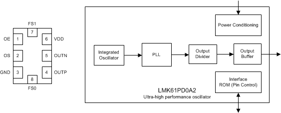
The LMK61PD0A2 is an ultra-low jitter PLLatinumTM pin selectable oscillator that generates commonly used reference clocks. The device is pre-programmed in factory to support seven unique reference clock frequencies that can be selected by pin-strapping each of FS[1:0] to VDD, GND or NC (no connect). Output format is selected between LVPECL, LVDS, or HCSL by pin-strapping OS to VDD, GND or NC. Internal power conditioning provide excellent power supply ripple rejection (PSRR), reducing the cost and complexity of the power delivery network. The device operates from a single 3.3 V ± 5% supply.
Device Information(1)
| PART NUMBER | PACKAGE | BODY SIZE (NOM) |
|---|---|---|
| LMK61PD0A2 | 8-pin QFM (SIA) | 7.0 mm x 5.0 mm |
- For all available packages, see the orderable addendum at the end of the data sheet.
Pinout and Simplified Block Diagram
