SNOSAR2H September   2008  – April 2016 LMP8601 , LMP8601-Q1 , LMP8602 , LMP8602-Q1 , LMP8603 , LMP8603-Q1

PRODUCTION DATA.  

  1. Features
  2. Applications
  3. Description
  4. Revision History
  5. Pin Configuration and Functions
  6. Specifications
    1. 6.1 Absolute Maximum Ratings
    2. 6.2 ESD Ratings: LMP860x
    3. 6.3 ESD Ratings: LMP860x-Q1
    4. 6.4 Recommended Operating Conditions
    5. 6.5 Thermal Information
    6. 6.6 Electrical Characteristics: VS = 3.3 V
    7. 6.7 Electrical Characteristics: VS = 5 V
    8. 6.8 Typical Characteristics
  7. Detailed Description
    1. 7.1 Overview
      1. 7.1.1 Theory of Operation
    2. 7.2 Functional Block Diagram
    3. 7.3 Feature Description
      1. 7.3.1 Offset Input Pin
      2. 7.3.2 Additional Second-Order Low-Pass Filter
    4. 7.4 Device Functional Modes
      1. 7.4.1 Gain Adjustment
        1. 7.4.1.1 Reducing Gain
        2. 7.4.1.2 Increasing Gain
      2. 7.4.2 Driving Switched Capacitive Loads
  8. Application and Implementation
    1. 8.1 Application Information
      1. 8.1.1 Specifying Performance
    2. 8.2 Typical Applications
      1. 8.2.1 High-Side, Current-Sensing Application
        1. 8.2.1.1 Design Requirements
        2. 8.2.1.2 Detailed Design Procedure
        3. 8.2.1.3 Application Curve
      2. 8.2.2 Low-Side, Current-Sensing Application
      3. 8.2.3 Battery Current Monitor Application
      4. 8.2.4 Advanced Battery Charger Application
      5. 8.2.5 Current Loop Receiver Application
  9. Power Supply Recommendations
  10. 10Layout
    1. 10.1 Layout Guidelines
    2. 10.2 Layout Example
  11. 11Device and Documentation Support
    1. 11.1 Device Support
      1. 11.1.1 Development Support
    2. 11.2 Related Links
    3. 11.3 Community Resources
    4. 11.4 Trademarks
    5. 11.5 Electrostatic Discharge Caution
    6. 11.6 Glossary
  12. 12Mechanical, Packaging, and Orderable Information

Package Options

Mechanical Data (Package|Pins)
Thermal pad, mechanical data (Package|Pins)
Orderable Information

5 Pin Configuration and Functions

D Package
8-Pin SOIC
Top View
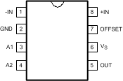
LMP8601 LMP8601-Q1 LMP8602 LMP8602-Q1 LMP8603 LMP8603-Q1 30083402.gif
DGK Package
8-Pin VSSOP
Top View
LMP8601 LMP8601-Q1 LMP8602 LMP8602-Q1 LMP8603 LMP8603-Q1 30083402.gif

Pin Descriptions

PIN TYPE DESCRIPTION
NAME NO.
A1 3 O Preamplifier output
A2 4 I Input from the external filter network and, or A1
GND 2 P Power ground
+IN 8 I Positive input
-IN 1 I Negative input
OFFSET 7 I DC offset for bidirectional signals
OUT 5 O Single-ended output
VS 6 P Positive supply voltage