SNOSC63B February   2012  – December 2014 LMP8646

PRODUCTION DATA.  

  1. Features
  2. Applications
  3. Description
    1.     Device Images
      1.      Typical Application
  4. Revision History
  5. Pin Configuration and Functions
    1.     Pin Functions
  6. Specifications
    1. 6.1 Absolute Maximum Ratings
    2. 6.2 ESD Ratings
    3. 6.3 Recommended Operating Conditions
    4. 6.4 Thermal Information
    5. 6.5 Electrical Characteristics: 2.7 V
    6. 6.6 Electrical Characteristics: 5 V
    7. 6.7 Electrical Characteristics: 12 V
    8. 6.8 Typical Characteristics
  7. Detailed Description
    1. 7.1 Overview
    2. 7.2 Functional Block Diagram
    3. 7.3 Feature Description
      1. 7.3.1 Theory of Operation
        1. 7.3.1.1 Maximum Output Voltage, VOUT_MAX
          1. 7.3.1.1.1 Case 1: −2 V < VCM < 1.8 V, and VS > 2.7 V
          2. 7.3.1.1.2 Case 2: 1.8 V < VCM < VS, and VS > 3.3 V
          3. 7.3.1.1.3 Case 3: VCM > VS, and VS > 2.7 V
    4. 7.4 Device Functional Modes
      1. 7.4.1 Output Accuracy
      2. 7.4.2 Selection of the Sense Resistor, RSENSE
        1. 7.4.2.1 RSENSE Consideration for System Error
  8. Application and Implementation
    1. 8.1 Application Information
    2. 8.2 Typical Applications
      1. 8.2.1 Application #1: Current Limiter With a Capacitive Load
        1. 8.2.1.1 Design Requirements
        2. 8.2.1.2 Detailed Design Procedure
        3. 8.2.1.3 Application Curve
      2. 8.2.2 Application #2: Current Limiter With a Resistive Load
        1. 8.2.2.1 Design Requirements
        2. 8.2.2.2 Detailed Design Procedure
        3. 8.2.2.3 Application Curve
      3. 8.2.3 Application #3: Current Limiter With a Low-Dropout Regulator and Resistive Load
        1. 8.2.3.1 Design Requirements
        2. 8.2.3.2 Detailed Design Procedure
        3. 8.2.3.3 Application Curve
  9. Power Supply Recommendations
  10. 10Layout
    1. 10.1 Layout Guidelines
    2. 10.2 Layout Example
  11. 11Device and Documentation Support
    1. 11.1 Trademarks
    2. 11.2 Electrostatic Discharge Caution
    3. 11.3 Glossary
  12. 12Mechanical, Packaging, and Orderable Information

Package Options

Mechanical Data (Package|Pins)
Thermal pad, mechanical data (Package|Pins)
Orderable Information

Output Accuracy

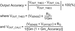
The output accuracy is the device error contributed by the LMP8646 based on its offset and gain errors. The LMP8646 output accuracy has the following equations:
Equation 7. LMP8646 30123538.gif
Output Accuracy Equations

For example, assume VSENSE = 100 mV, RG = 10 kOhm, and it is known that VOFFSET = 1 mV and Gm_Accuracy = 2% (Electrical Characteristics Table), then the output accuracy can be calculated as:

Equation 8. LMP8646 30123539.gif
Output Accuracy Example

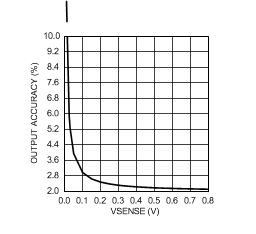
In fact, as VSENSE decreases, the output accuracy worsens as seen in Figure 27. These equations provide a valuable tool to estimate how the LMP8646 affects the overall system performance. Knowing this information allows the system designer to pick the appropriate external resistances (RSENSE and RG) to adjust for the tolerable system error. Examples of this tolerable system error can be seen in the next sections.
LMP8646 30123570.gifFigure 27. Output Accuracy vs. VSENSE