SNVSBP4C March 2020 – January 2021 LMQ61460-Q1
PRODUCTION DATA
- 1 Features
- 2 Applications
- 3 Description
- 4 Revision History
- 5 Description (continued)
- 6 Device Comparison Table
- 7 Pin Configuration and Functions
- 8 Specifications
-
9 Detailed Description
- 9.1 Overview
- 9.2 Functional Block Diagram
- 9.3
Feature Description
- 9.3.1 EN/SYNC Uses for Enable and VIN UVLO
- 9.3.2 EN/SYNC Pin Uses for Synchronization
- 9.3.3 Adjustable Switching Frequency
- 9.3.4 Clock Locking
- 9.3.5 PGOOD Output Operation
- 9.3.6 Internal LDO, VCC UVLO, and BIAS Input
- 9.3.7 Bootstrap Voltage and VCBOOT-UVLO (CBOOT Pin)
- 9.3.8 Adjustable SW Node Slew Rate
- 9.3.9 Spread Spectrum
- 9.3.10 Soft Start and Recovery From Dropout
- 9.3.11 Output Voltage Setting
- 9.3.12 Overcurrent and Short Circuit Protection
- 9.3.13 Thermal Shutdown
- 9.3.14 Input Supply Current
- 9.4 Device Functional Modes
-
10Application and Implementation
- 10.1 Application Information
- 10.2
Typical Application
- 10.2.1 Design Requirements
- 10.2.2
Detailed Design Procedure
- 10.2.2.1 Choosing the Switching Frequency
- 10.2.2.2 Setting the Output Voltage
- 10.2.2.3 Inductor Selection
- 10.2.2.4 Output Capacitor Selection
- 10.2.2.5 Input Capacitor Selection
- 10.2.2.6 BOOT Capacitor
- 10.2.2.7 BOOT Resistor
- 10.2.2.8 VCC
- 10.2.2.9 BIAS
- 10.2.2.10 CFF and RFF Selection
- 10.2.2.11 External UVLO
- 10.2.3 Application Curves
- 11Power Supply Recommendations
- 12Layout
- 13Device and Documentation Support
- 14Mechanical, Packaging, and Orderable Information
Package Options
Mechanical Data (Package|Pins)
- RJR|14
Thermal pad, mechanical data (Package|Pins)
Orderable Information
10.2.2.3 Inductor Selection
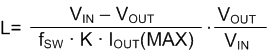
The parameters for selecting the inductor are the inductance and saturation current. The inductance is based on the desired peak-to-peak ripple current and is normally chosen to be in the range of 20% to 40% of the maximum output current. Experience shows that the best value for inductor ripple current is 30% of the maximum load current for systems with a fixed input voltage and 25% for systems with a variable input voltage such as the 12 volt battery in a car. Note that when selecting the ripple current for applications with much smaller maximum load than the maximum available from the device, the maximum device current must still be used. Equation 9 can be used to determine the value of inductance. The constant K is the percentage of inductor current ripple. For this example, K = 0.25 was chosen and an inductance of approximately 5.25 μH was found. The next standard value of 4.7 μH was selected.
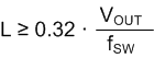
The saturation current rating of the inductor must be at least as large as the high-side switch current limit, IL-HS (see Section 8.5). This ensures that the inductor does not saturate even during a short circuit on the output. When the inductor core material saturates, the inductance falls to a very low value, causing the inductor current to rise very rapidly. Although the valley current limit, IL-LS, is designed to reduce the risk of current run-away, a saturated inductor can cause the current to rise to high values very rapidly. This can lead to component damage; do not allow the inductor to saturate. Inductors with a ferrite core material have very hard saturation characteristics, but usually have lower core losses than powdered iron cores. Powdered iron cores exhibit a soft saturation, allowing some relaxation in the current rating of the inductor. However, they have more core losses at frequencies typically above 1 MHz. In any case, the inductor saturation current must not be less than the device high-side current limit, IL-HS (see Section 8.5). To avoid subharmonic oscillation, the inductance value must not be less than that given in Equation 10. The maximum inductance is limited by the minimum current ripple required for the current mode control to perform correctly. As a rule-of-thumb, the minimum inductor ripple current must be no less than about 10% of the device maximum rated current under nominal conditions.
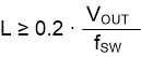
Equation 10 assumes that this design must operate with input voltage near or in dropout. If minimum operating voltage for this design is high enough to limit duty factor to below 50%, Equation 11 can be used in place of Equation 10.
Note that choosing an inductor that is larger than the minimum inductance calculated using Equation 9 through Equation 11 results in less output capacitance being needed to limit output ripple but more output capacitance being needed to manage large load transients. See Section 10.2.2.4.