SNVSBR8D March 2020 – June 2022 LMQ61460
PRODUCTION DATA
- 1 Features
- 2 Applications
- 3 Description
- 4 Revision History
- 5 Device Comparison Table
- 6 Pin Configuration and Functions
- 7 Specifications
-
8 Detailed Description
- 8.1 Overview
- 8.2 Functional Block Diagram
- 8.3
Feature Description
- 8.3.1 EN/SYNC Uses for Enable and VIN UVLO
- 8.3.2 EN/SYNC Pin Uses for Synchronization
- 8.3.3 Adjustable Switching Frequency
- 8.3.4 Clock Locking
- 8.3.5 PGOOD Output Operation
- 8.3.6 Internal LDO, VCC UVLO, and BIAS Input
- 8.3.7 Bootstrap Voltage and VCBOOT-UVLO (CBOOT Pin)
- 8.3.8 Adjustable SW Node Slew Rate
- 8.3.9 Spread Spectrum
- 8.3.10 Soft Start and Recovery From Dropout
- 8.3.11 Output Voltage Setting
- 8.3.12 Overcurrent and Short Circuit Protection
- 8.3.13 Thermal Shutdown
- 8.3.14 Input Supply Current
- 8.4 Device Functional Modes
- 9 Application and Implementation
- 10Power Supply Recommendations
- 11Layout
- 12Device and Documentation Support
- 13Mechanical, Packaging, and Orderable Information
Package Options
Mechanical Data (Package|Pins)
- RJR|14
Thermal pad, mechanical data (Package|Pins)
Orderable Information
9.2.2.11 External UVLO
In some cases, an input UVLO level different than that provided internal to the device is needed, which can be accomplished by using the circuit shown in Figure 9-4. The input voltage at which the device turns on is designated VON while the turn-off voltage is VOFF. First, a value for RENB is chosen in the range of 10 kΩ to 100 kΩ, then Equation 14 is used to calculate RENT and VOFF. RENB is typically set based on how much current this voltage divider must consume. RENB can be calculated using Equation 13.
Equation 13. 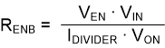
 Figure 9-4 UVLO
Using EN
Figure 9-4 UVLO
Using ENEquation 14. 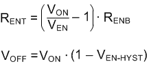
where
- VON is VIN turn-on voltage.
- VOFF is VIN turn-off voltage.
- IDIVIDER is voltage divider current.