SNVS728D October   2011  – June 2019 LMR10515

PRODUCTION DATA.  

  1. Features
  2. Applications
  3. Description
    1.     Device Images
      1.      Simplified Application
  4. Revision History
  5. Description, continued
  6. Pin Configuration and Functions
    1.     Pin Description: 5-Pin SOT-23
    2.     Pin Descriptions 6-Pin WSON
  7. Specifications
    1. 7.1 Absolute Maximum Ratings
    2. 7.2 Recommended Operating Ratings
    3. 7.3 Electrical Characteristics
    4. 7.4 Typical Characteristics
  8. Detailed Description
    1. 8.1 Overview
    2. 8.2 Functional Block Diagram
    3. 8.3 Feature Description
      1. 8.3.1 Soft-Start
      2. 8.3.2 Output Overvoltage Protection
      3. 8.3.3 Undervoltage Lockout
      4. 8.3.4 Current Limit
      5. 8.3.5 Thermal Shutdown
  9. Application and Implementation
    1. 9.1 Application Information
    2. 9.2 Typical Application
      1. 9.2.1 Detailed Design Procedure
        1. 9.2.1.1 Custom Design With WEBENCH® Tools
        2. 9.2.1.2 Inductor Selection
        3. 9.2.1.3 Input Capacitor
        4. 9.2.1.4 Output Capacitor
        5. 9.2.1.5 Catch Diode
        6. 9.2.1.6 Output Voltage
        7. 9.2.1.7 Calculating Efficiency, And Junction Temperature
      2. 9.2.2 Application Curves
      3. 9.2.3 Other System Examples
        1. 9.2.3.1 LMR10510x Design Example 1
        2. 9.2.3.2 Lmr10510X Design Example 2
        3. 9.2.3.3 LMR10510Y Design Example 3
        4. 9.2.3.4 LMR10510Y Design Example 4
  10. 10Layout
    1. 10.1 Layout Guidelines
    2. 10.2 Layout Example
    3. 10.3 Thermal Definitions
    4. 10.4 WSON Package
  11. 11Device and Documentation Support
    1. 11.1 Device Support
      1. 11.1.1 Development Support
        1. 11.1.1.1 Custom Design With WEBENCH® Tools
    2. 11.2 Receiving Notification of Documentation Updates
    3. 11.3 Community Resources
    4. 11.4 Trademarks
    5. 11.5 Electrostatic Discharge Caution
    6. 11.6 Glossary
  12. 12Mechanical, Packaging, and Orderable Information

Package Options

Mechanical Data (Package|Pins)
Thermal pad, mechanical data (Package|Pins)
Orderable Information

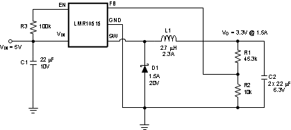
Lmr10510X Design Example 2

LMR10515 30166160.gifFigure 23. LMR10510X (1.6 MHz): VIN = 5 V, VOUT = 3.3 V at 1 A