SNVS817B June 2012 – June 2019 LMR12015 , LMR12020
PRODUCTION DATA.
- 1 Features
- 2 Applications
- 3 Description
- 4 Revision History
- 5 Pin Configuration and Functions
- 6 Specifications
- 7 Detailed Description
-
8 Application and Implementation
- 8.1 Application Information
- 8.2
Typical Application
- 8.2.1
Detailed Design Procedure
- 8.2.1.1 Custom Design With WEBENCH® Tools
- 8.2.1.2 Inductor Selection
- 8.2.1.3 Input Capacitor
- 8.2.1.4 Output Capacitor
- 8.2.1.5 Catch Diode
- 8.2.1.6 Boost Diode (Optional)
- 8.2.1.7 Boost Capacitor
- 8.2.1.8 Output Voltage
- 8.2.1.9 Feedforward Capacitor (Optional)
- 8.2.1.10
Calculating Efficiency and Junction Temperature
- 8.2.1.10.1 Schottky Diode Conduction Losses
- 8.2.1.10.2 Inductor Conduction Losses
- 8.2.1.10.3 MOSFET Conduction Losses
- 8.2.1.10.4 MOSFET Switching Losses
- 8.2.1.10.5 IC Quiescent Losses
- 8.2.1.10.6 MOSFET Driver Losses
- 8.2.1.10.7 Total Power Losses
- 8.2.1.10.8 Efficiency Calculation Example
- 8.2.1.10.9 Calculating the LMR2015/20 Junction Temperature
- 8.2.2 Application Curves
- 8.2.3 LMR12015/20 Circuit Examples
- 8.2.1
Detailed Design Procedure
- 9 Layout
- 10Device and Documentation Support
- 11Mechanical, Packaging, and Orderable Information
Package Options
Mechanical Data (Package|Pins)
- DSC|10
Thermal pad, mechanical data (Package|Pins)
- DSC|10
Orderable Information
8.2.1.10.9 Calculating the LMR2015/20 Junction Temperature
Thermal Definitions:
TJ = IC junction temperature
TA = Ambient temperature
RθJC = Thermal resistance from IC junction to device case
RθJA = Thermal resistance from IC junction to ambient air
 Figure 30. Cross-Sectional View Of Integrated Circuit Mounted On A Printed Circuit Board.
 Heat in the LMR12015/20 due to internal power dissipation is removed through conduction and/or convection.
Conduction: Heat transfer occurs through cross sectional areas of material. Depending on the material, the transfer of heat can be considered to have poor to good thermal conductivity properties (insulator vs conductor).
Heat Transfer goes as:
Convection: Heat transfer is by means of airflow. This could be from a fan or natural convection. Natural convection occurs when air currents rise from the hot device to cooler air.
Thermal impedance is defined as:

Thermal impedance from the silicon junction to the ambient air is defined as:

This impedance can vary depending on the thermal properties of the PCB. This includes PCB size, weight of copper used to route traces , the ground plane, and the number of layers within the PCB. The type and number of thermal vias can also make a large difference in the thermal impedance. Thermal vias are necessary in most applications. They conduct heat from the surface of the PCB to the ground plane. Six to nine thermal vias should be placed under the exposed pad to the ground plane. Placing more than nine thermal vias results in only a small reduction to RθJA for the same copper area. These vias should have 8 mil holes to avoid wicking solder away from the DAP. See AN-1187 Leadless Leadframe Package (LLP)and AN-1520 A Guide to Board Layout for Best Thermal Resistance for Exposed Packages for more information on package thermal performance.
To predict the silicon junction temperature for a given application, three methods can be used. The first is useful before prototyping and the other two can more accurately predict the junction temperature within the application.
Method 1:
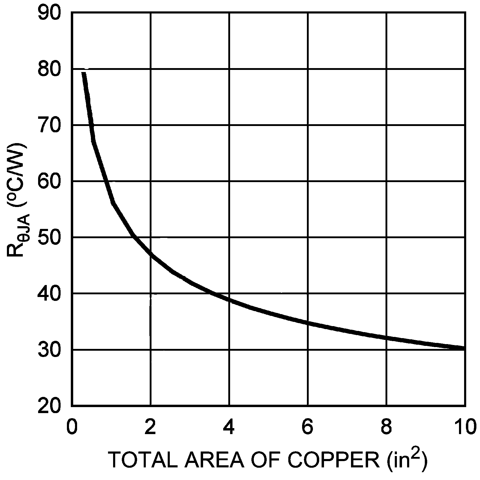
The first method predicts the junction temperature by extrapolating a best guess RθJA from the table or graph. The tables and graph are for natural convection. The internal dissipation can be calculated using the efficiency calculations. This allows the user to make a rough prediction of the junction temperature in their application. Methods two and three can later be used to determine the junction temperature more accurately.
The table below has values of RθJA for the WSON package.
Table 2. RθJAValues for the WSON at 1-Watt Dissipation:
| NUMBER OF BOARD LAYERS | SIZE OF BOTTOM LAYER COPPER CONNECTED TO DAP | SIZE OF TOP LAYER COPPER CONNECTED TO DAP | NUMBER OF 8 MIL THERMAL VIAS | RθJA |
| 2 | 0.25 in2 | 0.05 in2 | 8 | 78°C/W |
| 2 | 0.5625 in2 | 0.05 in2 | 8 | 65.6°C/W |
| 2 | 1 in2 | 0.05 in2 | 8 | 58.6°C/W |
| 2 | 1.3225 in2 | 0.05 in2 | 8 | 50°C/W |
| 4 (Eval Board) | 3.25 in2 | 2.25 in2 | 15 | 30.7°C/W |
 Figure 31. Estimate of Thermal Resistance vs. Ground Copper Area
Eight Thermal Vias and Natural Convection
Method 2:
The second method requires the user to know the thermal impedance of the silicon junction to case. (RθJC) is approximately 9.1°C/W for the WSON. The case temperature should be measured on the bottom of the PCB at a thermal via directly under the DAP of the LMR12015/20. The solder resist must be removed from this area for temperature testing. The reading will be more accurate if it is taken midway between pins 2 and 9, where the NMOS switch is located. Knowing the internal dissipation from the efficiency calculation given previously, and the case temperature (TC) we have:

Therefore: