SNVSAH9B December 2015 – March 2021 LMR16030
PRODUCTION DATA
- 1 Features
- 2 Applications
- 3 Description
- 4 Revision History
- 5 Pin Configuration and Functions
- 6 Specifications
-
7 Detailed Description
- 7.1 Overview
- 7.2 Functional Block Diagram
- 7.3
Feature Description
- 7.3.1 Fixed Frequency Peak Current Mode Control
- 7.3.2 Slope Compensation
- 7.3.3 Sleep Mode
- 7.3.4 Low Dropout Operation and Bootstrap Voltage (BOOT)
- 7.3.5 Adjustable Output Voltage
- 7.3.6 Enable and Adjustable Undervoltage Lockout
- 7.3.7 External Soft Start
- 7.3.8 Switching Frequency and Synchronization (RT/SYNC)
- 7.3.9 Power Good (PGOOD)
- 7.3.10 Overcurrent and Short Circuit Protection
- 7.3.11 Overvoltage Protection
- 7.3.12 Thermal Shutdown
- 7.4 Device Functional Modes
- 8 Application and Implementation
- 9 Power Supply Recommendations
- 10Layout
- 11Device and Documentation Support
- 12Mechanical, Packaging, and Orderable Information
Package Options
Mechanical Data (Package|Pins)
- DDA|8
Thermal pad, mechanical data (Package|Pins)
- DDA|8
Orderable Information
8.2.2.5 Output Capacitor Selection
The output capacitor or capacitors, COUT, must be chosen with care since it directly affects the steady state output voltage ripple, loop stability and the voltage overshoot and undershoot during load current transients.
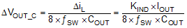
The output ripple is essentially composed of two parts. One is caused by the inductor current ripple going through the Equivalent Series Resistance (ESR) of the output capacitors:

The other is caused by the inductor current ripple charging and discharging the output capacitors:
The two components in the voltage ripple are not in phase, so the actual peak-to-peak ripple is smaller than the sum of two peaks.
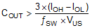
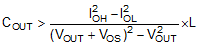
Output capacitance is usually limited by transient performance specifications if the system requires tight voltage regulation with presence of large current steps and fast slew rate. When a fast large load increase happens, output capacitors provide the required charge before the inductor current can slew up to the appropriate level. The control loop of the regulator usually needs three or more clock cycles to respond to the output voltage droop. The output capacitance must be large enough to supply the current difference for three clock cycles to maintain the output voltage within the specified range. Equation 13 shows the minimum output capacitance needed for specified output undershoot. When a sudden large load decrease happens, the output capacitors absorb energy stored in the inductor. The catch diode cannot sink current so the energy stored in the inductor results in an output voltage overshoot. Equation 14 calculates the minimum capacitance required to keep the voltage overshoot within a specified range.
where
- KIND = Ripple ratio of the inductor ripple current (ΔiL / IOUT)
- IOL = Low level output current during load transient
- IOH = High level output current during load transient
- VUS = Target output voltage undershoot
- VOS = Target output voltage overshoot
For this design example, the target output ripple is 50 mV. Presuppose ΔVOUT_ESR = ΔVOUT_C = 50 mV, and chose KIND = 0.4. Equation 11 yields ESR no larger than 41.7 mΩ and Equation 12 yields COUT no smaller than 6 μF. For the target overshoot and undershoot range of this design, VUS = VOS = 5% × VOUT = 250 mV. The COUT can be calculated to be no smaller than 64.8 μF and 6.4 μF by Equation 13 and Equation 14 respectively. In summary, the most stringent criteria for the output capacitor is 100 μF. For this design example, two 47-μF, 16-V, X7R ceramic capacitors with 5-mΩ ESR are used in parallel.