SNVSAH2E December 2015 – August 2020 LMR23630
PRODUCTION DATA
- 1 Features
- 2 Applications
- 3 Description
- 4 Revision History
- 5 Device Comparison Table
- 6 Pin Configuration and Functions
- 7 Specifications
-
8 Detailed Description
- 8.1 Overview
- 8.2 Functional Block Diagram
- 8.3
Feature Description
- 8.3.1 Fixed Frequency Peak Current Mode Control
- 8.3.2 Adjustable Frequency
- 8.3.3 Adjustable Output Voltage
- 8.3.4 Enable/Sync
- 8.3.5 VCC, UVLO
- 8.3.6 Minimum ON-time, Minimum OFF-time and Frequency Foldback at Dropout Conditions
- 8.3.7 Power Good (PGOOD)
- 8.3.8 Internal Compensation and CFF
- 8.3.9 Bootstrap Voltage (BOOT)
- 8.3.10 Overcurrent and Short-Circuit Protection
- 8.3.11 Thermal Shutdown
- 8.4 Device Functional Modes
-
9 Application and Implementation
- 9.1 Application Information
- 9.2
Typical Applications
- 9.2.1 Design Requirements
- 9.2.2
Detailed Design Procedure
- 9.2.2.1 Custom Design With WEBENCH® Tools
- 9.2.2.2 Output Voltage Setpoint
- 9.2.2.3 Switching Frequency
- 9.2.2.4 Inductor Selection
- 9.2.2.5 Output Capacitor Selection
- 9.2.2.6 Feed-Forward Capacitor
- 9.2.2.7 Input Capacitor Selection
- 9.2.2.8 Bootstrap Capacitor Selection
- 9.2.2.9 VCC Capacitor Selection
- 9.2.2.10 Undervoltage Lockout Setpoint
- 9.2.3 Application Curves
- 10Power Supply Recommendations
- 11Layout
- 12Device and Documentation Support
- 13Mechanical, Packaging, and Orderable Information
Package Options
Refer to the PDF data sheet for device specific package drawings
Mechanical Data (Package|Pins)
- DDA|8
- DRR|12
Thermal pad, mechanical data (Package|Pins)
Orderable Information
8.3.6 Minimum ON-time, Minimum OFF-time and Frequency Foldback at Dropout Conditions
Minimum ON-time, TON_MIN, is the smallest duration of time that the HS switch can be on. TON_MIN is typically 60 ns in the LMR23630. Minimum OFF-time, TOFF_MIN, is the smallest duration that the HS switch can be off. TOFF_MIN is typically 100 ns in the LMR23630. In CCM operation, TON_MIN and TOFF_MIN limit the voltage conversion range given a selected switching frequency.
The minimum duty cycle allowed is:
And the maximum duty cycle allowed is:
Given fixed TON_MIN and TOFF_MIN, the higher the switching frequency the narrower the range of the allowed duty cycle. In the LMR23630, a frequency foldback scheme is employed to extend the maximum duty cycle when TOFF_MIN is reached. The switching frequency decreases once longer duty cycle is needed under low VIN conditions. Wide range of frequency foldback allows the LMR23630 output voltage stay in regulation with a much lower supply voltage VIN. This leads to a lower effective dropout voltage.
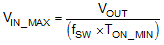
Given an output voltage, the choice of the switching frequency affects the allowed input voltage range, solution size and efficiency. The maximum operation supply voltage can be found by:
At lower supply voltage, the switching frequency decreases once TOFF_MIN is tripped. The minimum VIN without frequency foldback can be approximated by:
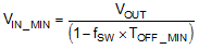
Taking considerations of power losses in the system with heavy load operation, VIN_MAX is higher than the result calculated in Equation 5. With frequency foldback, VIN_MIN is lowered by decreased fSW.
") Figure 8-8 Frequency Foldback at Dropout (VOUT = 5 V, fSW = 400 kHz)
Figure 8-8 Frequency Foldback at Dropout (VOUT = 5 V, fSW = 400 kHz)