SNVSAH2E December 2015 – August 2020 LMR23630
PRODUCTION DATA
- 1 Features
- 2 Applications
- 3 Description
- 4 Revision History
- 5 Device Comparison Table
- 6 Pin Configuration and Functions
- 7 Specifications
-
8 Detailed Description
- 8.1 Overview
- 8.2 Functional Block Diagram
- 8.3
Feature Description
- 8.3.1 Fixed Frequency Peak Current Mode Control
- 8.3.2 Adjustable Frequency
- 8.3.3 Adjustable Output Voltage
- 8.3.4 Enable/Sync
- 8.3.5 VCC, UVLO
- 8.3.6 Minimum ON-time, Minimum OFF-time and Frequency Foldback at Dropout Conditions
- 8.3.7 Power Good (PGOOD)
- 8.3.8 Internal Compensation and CFF
- 8.3.9 Bootstrap Voltage (BOOT)
- 8.3.10 Overcurrent and Short-Circuit Protection
- 8.3.11 Thermal Shutdown
- 8.4 Device Functional Modes
-
9 Application and Implementation
- 9.1 Application Information
- 9.2
Typical Applications
- 9.2.1 Design Requirements
- 9.2.2
Detailed Design Procedure
- 9.2.2.1 Custom Design With WEBENCH® Tools
- 9.2.2.2 Output Voltage Setpoint
- 9.2.2.3 Switching Frequency
- 9.2.2.4 Inductor Selection
- 9.2.2.5 Output Capacitor Selection
- 9.2.2.6 Feed-Forward Capacitor
- 9.2.2.7 Input Capacitor Selection
- 9.2.2.8 Bootstrap Capacitor Selection
- 9.2.2.9 VCC Capacitor Selection
- 9.2.2.10 Undervoltage Lockout Setpoint
- 9.2.3 Application Curves
- 10Power Supply Recommendations
- 11Layout
- 12Device and Documentation Support
- 13Mechanical, Packaging, and Orderable Information
Package Options
Refer to the PDF data sheet for device specific package drawings
Mechanical Data (Package|Pins)
- DDA|8
- DRR|12
Thermal pad, mechanical data (Package|Pins)
Orderable Information
9.2.2.4 Inductor Selection
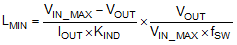
The most critical parameters for the inductor are the inductance, saturation current, and the rated current. The inductance is based on the desired peak-to-peak ripple current ΔiL. Because the ripple current increases with the input voltage, the maximum input voltage is always used to calculate the minimum inductance LMIN. Use Equation 12 to calculate the minimum value of the output inductor. KIND is a coefficient that represents the amount of inductor ripple current relative to the maximum output current of the device. A reasonable value of KIND should be 20% to 40%. During an instantaneous short or overcurrent operation event, the RMS and peak inductor current can be high. The inductor current rating should be higher than the current limit of the device.
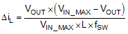
In general, it is preferable to choose lower inductance in switching power supplies, because it usually corresponds to faster transient response, smaller DCR, and reduced size for more compact designs. However, inductance that is too low can generate an inductor current ripple that is too high so that overcurrent protection at the full load could be falsely triggered. It also generates more conduction loss and inductor core loss. Larger inductor current ripple also implies larger output voltage ripple with same output capacitors. With peak current mode control, TI does not recommend having an inductor current ripple that is too small. A larger peak-current ripple improves the comparator signal-to-noise ratio.
For this design example, choose KIND = 0.4, the minimum inductor value is calculated to be 8.56 µH. Choose the nearest standard 8.2 μH ferrite inductor with a capability of 4-A RMS current and 6-A saturation current.