SNVSAH2E December 2015 – August 2020 LMR23630
PRODUCTION DATA
- 1 Features
- 2 Applications
- 3 Description
- 4 Revision History
- 5 Device Comparison Table
- 6 Pin Configuration and Functions
- 7 Specifications
-
8 Detailed Description
- 8.1 Overview
- 8.2 Functional Block Diagram
- 8.3
Feature Description
- 8.3.1 Fixed Frequency Peak Current Mode Control
- 8.3.2 Adjustable Frequency
- 8.3.3 Adjustable Output Voltage
- 8.3.4 Enable/Sync
- 8.3.5 VCC, UVLO
- 8.3.6 Minimum ON-time, Minimum OFF-time and Frequency Foldback at Dropout Conditions
- 8.3.7 Power Good (PGOOD)
- 8.3.8 Internal Compensation and CFF
- 8.3.9 Bootstrap Voltage (BOOT)
- 8.3.10 Overcurrent and Short-Circuit Protection
- 8.3.11 Thermal Shutdown
- 8.4 Device Functional Modes
-
9 Application and Implementation
- 9.1 Application Information
- 9.2
Typical Applications
- 9.2.1 Design Requirements
- 9.2.2
Detailed Design Procedure
- 9.2.2.1 Custom Design With WEBENCH® Tools
- 9.2.2.2 Output Voltage Setpoint
- 9.2.2.3 Switching Frequency
- 9.2.2.4 Inductor Selection
- 9.2.2.5 Output Capacitor Selection
- 9.2.2.6 Feed-Forward Capacitor
- 9.2.2.7 Input Capacitor Selection
- 9.2.2.8 Bootstrap Capacitor Selection
- 9.2.2.9 VCC Capacitor Selection
- 9.2.2.10 Undervoltage Lockout Setpoint
- 9.2.3 Application Curves
- 10Power Supply Recommendations
- 11Layout
- 12Device and Documentation Support
- 13Mechanical, Packaging, and Orderable Information
Package Options
Refer to the PDF data sheet for device specific package drawings
Mechanical Data (Package|Pins)
- DDA|8
- DRR|12
Thermal pad, mechanical data (Package|Pins)
Orderable Information
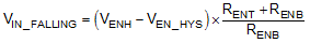
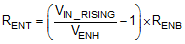
9.2.2.10 Undervoltage Lockout Setpoint
The system undervoltage lockout (UVLO) is adjusted using the external voltage divider network of RENT and RENB. The UVLO has two thresholds, one for power up when the input voltage is rising and one for power down or brown outs when the input voltage is falling. The following equation can be used to determine the VIN UVLO level.
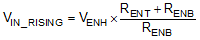
The EN rising threshold (VENH) for LMR23630 is set to be 1.55 V (typical). Choose the value of RENB to be 287 kΩ to minimize input current from the supply. If the desired VIN UVLO level is at 6 V, then the value of RENT can be calculated using Equation 21:
Equation 21 yields a value of 820 kΩ. The resulting falling UVLO threshold, equals 4.4 V, can be calculated by Equation 22, where EN hysteresis (VEN_HYS) is 0.4 V (typical).