SNVSAN3F August 2017 – November 2020 LMR33630
PRODUCTION DATA
- 1 Features
- 2 Applications
- 3 Description
- 4 Revision History
- 5 Device Comparison Table
- 6 Pin Configuration and Functions
- 7 Specifications
- 8 Detailed Description
-
9 Application and Implementation
- 9.1 Application Information
- 9.2
Typical Application
- 9.2.1 Design Requirements
- 9.2.2
Detailed Design Procedure
- 9.2.2.1 Custom Design With WEBENCH® Tools
- 9.2.2.2 Choosing the Switching Frequency
- 9.2.2.3 Setting the Output Voltage
- 9.2.2.4 Inductor Selection
- 9.2.2.5 Output Capacitor Selection
- 9.2.2.6 Input Capacitor Selection
- 9.2.2.7 CBOOT
- 9.2.2.8 VCC
- 9.2.2.9 CFF Selection
- 9.2.2.10 External UVLO
- 9.2.2.11 Maximum Ambient Temperature
- 9.2.3 Application Curves
- 9.3 What to Do and What Not to Do
- 10Layout
- 11Device and Documentation Support
Package Options
Refer to the PDF data sheet for device specific package drawings
Mechanical Data (Package|Pins)
- RNX|12
- DDA|8
Thermal pad, mechanical data (Package|Pins)
Orderable Information
3 Description
The LMR33630 SIMPLE SWITCHER® regulator is an easy-to-use, synchronous, step-down DC/DC converter that delivers best-in-class efficiency for rugged industrial applications. The LMR33630 drives up to 3 A of load current from an input of up to 36 V. The LMR33630 provides high light load efficiency and output accuracy in a very small solution size. Features such as a power-good flag and precision enable provide both flexible and easy-to-use solutions for a wide range of applications. The LMR33630 automatically folds back frequency at light load to improve efficiency. Integration eliminates most external components and provides a pinout designed for simple PCB layout. Protection features include thermal shutdown, input undervoltage lockout, cycle-by-cycle current limit, and hiccup short-circuit protection. The LMR33630 is available in an 8-pin HSOIC package and in a 12-pin 3 mm × 2 mm next generation VQFN package with wettable flanks. This device is also available in an AEC-Q100-qualified version.
| PART NUMBER | PACKAGE(1) | BODY SIZE (NOM) |
|---|---|---|
| LMR33630 | HSOIC (8) | 5.00 mm × 4.00 mm |
| LMR33630 | VQFN (12) | 3.00 mm × 2.00 mm |
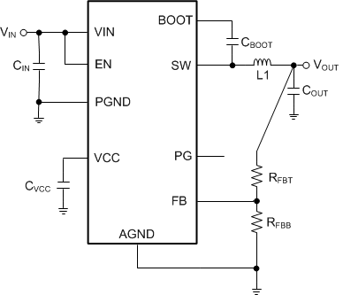
 Simplified Schematic
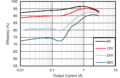
 Efficiency versus Output
Current VOUT = 5 V, 400 kHz, VQFN