SNVSB91C July 2019 – June 2020 LMR36506-Q1
PRODUCTION DATA.
- 1 Features
- 2 Applications
- 3 Description
- 4 Revision History
- 5 Device Comparison Table
- 6 Pin Configuration and Functions
- 7 Specifications
-
8 Detailed Description
- 8.1 Overview
- 8.2 Functional Block Diagram
- 8.3
Feature Description
- 8.3.1 Enable, Start-up and Shutdown
- 8.3.2 External CLK SYNC (with MODE/SYNC)
- 8.3.3 Adjustable Switching Frequency (with RT)
- 8.3.4 Power-Good Output Operation
- 8.3.5 Internal LDO, VCC UVLO, and VOUT/BIAS Input
- 8.3.6 Bootstrap Voltage and VCBOOT-UVLO (CBOOT Terminal)
- 8.3.7 Output Voltage Selection
- 8.3.8 Spread Spectrum
- 8.3.9 Soft Start and Recovery from Dropout
- 8.3.10 Current Limit and Short Circuit
- 8.3.11 Thermal Shutdown
- 8.3.12 Input Supply Current
- 8.4 Device Functional Modes
-
9 Application and Implementation
- 9.1 Application Information
- 9.2
Typical Application
- 9.2.1 Design Requirements
- 9.2.2 Detailed Design Procedure
- 9.2.3 Application Curves
- 9.3 What to Do and What Not to Do
- 10Power Supply Recommendations
- 11Layout
- 12Device and Documentation Support
- 13Mechanical, Packaging, and Orderable Information
Package Options
Mechanical Data (Package|Pins)
- RPE|9
Thermal pad, mechanical data (Package|Pins)
- RPE|9
Orderable Information
8.4.3.1 CCM Mode
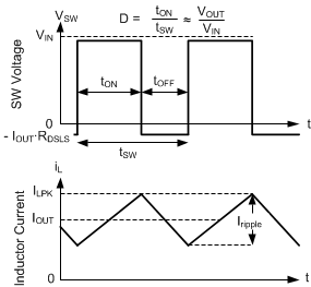
The following operating description of the LMR36506-Q1 refers to the Functional Block Diagram and to the waveforms in Figure 23. In CCM, the LMR36506-Q1 supplies a regulated output voltage by turning on the internal high-side (HS) and low-side (LS) switches with varying duty cycle (D). During the HS switch on-time, the SW pin voltage, VSW, swings up to approximately VIN, and the inductor current, iL, increases with a linear slope. The HS switch is turned off by the control logic. During the HS switch off-time, tOFF, the LS switch is turned on. Inductor current discharges through the LS switch, which forces the VSW to swing below ground by the voltage drop across the LS switch. The converter loop adjusts the duty cycle to maintain a constant output voltage. D is defined by the on-time of the HS switch over the switching period:
In an ideal buck converter where losses are ignored, D is proportional to the output voltage and inversely proportional to the input voltage:
 Figure 23. SW Voltage and Inductor Current Waveforms in Continuous Conduction Mode (CCM)