SNVSBB6B December 2019 – December 2022 LMR36506
PRODUCTION DATA
- 1 Features
- 2 Applications
- 3 Description
- 4 Revision History
- 5 Device Comparison Table
- 6 Pin Configuration and Functions
- 7 Specifications
-
8 Detailed Description
- 8.1 Overview
- 8.2 Functional Block Diagram
- 8.3
Feature Description
- 8.3.1 Enable, Start-up, and Shutdown
- 8.3.2 Adjustable Switching Frequency (with RT)
- 8.3.3 Power-Good Output Operation
- 8.3.4 Internal LDO, VCC UVLO, and VOUT/BIAS Input
- 8.3.5 Bootstrap Voltage and VCBOOT-UVLO (CBOOT Terminal)
- 8.3.6 Output Voltage Selection
- 8.3.7 Soft Start and Recovery from Dropout
- 8.3.8 Current Limit and Short Circuit
- 8.3.9 Thermal Shutdown
- 8.3.10 Input Supply Current
- 8.4 Device Functional Modes
-
9 Application and Implementation
- 9.1 Application Information
- 9.2
Typical Application
- 9.2.1 Design Requirements
- 9.2.2 Detailed Design Procedure
- 9.2.3 Application Curves
- 9.3 Best Design Practices
- 9.4 Power Supply Recommendations
- 9.5 Layout
- 10Device and Documentation Support
- 11Mechanical, Packaging, and Orderable Information
Package Options
Mechanical Data (Package|Pins)
- RPE|9
Thermal pad, mechanical data (Package|Pins)
- RPE|9
Orderable Information
9.2.2.3 Inductor Selection
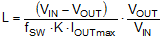
The parameters for selecting the inductor are the inductance and saturation current. The inductance is based on the desired peak-to-peak ripple current and is normally chosen to be in the range of 20% to 40% of the maximum output current. Experience shows that the best value for inductor ripple current is 30% of the maximum load current. Note that when selecting the ripple current for applications with much smaller maximum load than the maximum available from the device, use the maximum device current. Equation 7 can be used to determine the value of inductance. The constant K is the percentage of inductor current ripple. For this example, choose K = 0.3 and find an inductance of L = 22 µH. Select the next standard value of L = 22 µH.
Ideally, the saturation current rating of the inductor is at least as large as the high-side switch current limit, ISC (see Section 7.5). This ensures that the inductor does not saturate, even during a short circuit on the output. When the inductor core material saturates, the inductance falls to a very low value, causing the inductor current to rise very rapidly. Although the valley current limit, ILIMIT, is designed to reduce the risk of current runaway, a saturated inductor can cause the current to rise to high values very rapidly. This can lead to component damage. Do not allow the inductor to saturate. Inductors with a ferrite core material have very hard saturation characteristics, but usually have lower core losses than powdered iron cores. Powered iron cores exhibit a soft saturation, allowing some relaxation in the current rating of the inductor. However, they have more core losses at frequencies above about 1 MHz. In any case, the inductor saturation current must not be less than the maximum peak inductor current at full load.
To avoid subharmonic oscillation, the inductance value must not be less than that given in Equation 8:
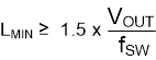
The maximum inductance is limited by the minimum current ripple for the current mode control to perform correctly. As a rule-of-thumb, the minimum inductor ripple current must be no less than about 10% of the device maximum rated current under nominal conditions.