SNVSBB6B December 2019 – December 2022 LMR36506
PRODUCTION DATA
- 1 Features
- 2 Applications
- 3 Description
- 4 Revision History
- 5 Device Comparison Table
- 6 Pin Configuration and Functions
- 7 Specifications
-
8 Detailed Description
- 8.1 Overview
- 8.2 Functional Block Diagram
- 8.3
Feature Description
- 8.3.1 Enable, Start-up, and Shutdown
- 8.3.2 Adjustable Switching Frequency (with RT)
- 8.3.3 Power-Good Output Operation
- 8.3.4 Internal LDO, VCC UVLO, and VOUT/BIAS Input
- 8.3.5 Bootstrap Voltage and VCBOOT-UVLO (CBOOT Terminal)
- 8.3.6 Output Voltage Selection
- 8.3.7 Soft Start and Recovery from Dropout
- 8.3.8 Current Limit and Short Circuit
- 8.3.9 Thermal Shutdown
- 8.3.10 Input Supply Current
- 8.4 Device Functional Modes
-
9 Application and Implementation
- 9.1 Application Information
- 9.2
Typical Application
- 9.2.1 Design Requirements
- 9.2.2 Detailed Design Procedure
- 9.2.3 Application Curves
- 9.3 Best Design Practices
- 9.4 Power Supply Recommendations
- 9.5 Layout
- 10Device and Documentation Support
- 11Mechanical, Packaging, and Orderable Information
Package Options
Mechanical Data (Package|Pins)
- RPE|9
Thermal pad, mechanical data (Package|Pins)
- RPE|9
Orderable Information
9.2.2.9 Maximum Ambient Temperature
As with any power conversion device, the LMR36506 dissipates internal power while operating. The effect of this power dissipation is to raise the internal temperature of the converter above ambient. The internal die temperature (TJ) is a function of the ambient temperature, the power loss, and the effective thermal resistance, RθJA, of the device and PCB combination. The maximum junction temperature for the LMR36506 must be limited to 150°C. This establishes a limit on the maximum device power dissipation and, therefore, the load current. Equation 12 shows the relationships between the important parameters. Larger ambient temperatures (TA) and larger values of RθJA reduce the maximum available output current. The converter efficiency can be estimated by using the curves provided in this data sheet. If the desired operating conditions cannot be found in one of the curves, interpolation can be used to estimate the efficiency. Alternatively, the EVM can be adjusted to match the desired application requirements and the efficiency can be measured directly. The correct value of RθJA is more difficult to estimate. As stated in the Semiconductor and IC Package Thermal Metrics Application Report, the values given in Section 7.4 are not valid for design purposes and must not be used to estimate the thermal performance of the application. The values reported in that table were measured under a specific set of conditions that are rarely obtained in an actual application.
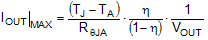
where
- η is the efficiency.
The effective RθJA is a critical parameter and depends on many factors such as the following:
- Power dissipation
- Air temperature/flow
- PCB area
- Copper heat-sink area
- Number of thermal vias under the package
- Adjacent component placement
A typical example of RθJA versus copper board area can be found in Figure 9-3. The copper area given in the graph is for each layer. For a 4-layer PCB design, the top and bottom layers are 2-oz. copper each, while the inner layers are 1 oz. For a 2-layer PCB design, the top and bottom layers are 2-oz. copper each. Note that the data given in these graphs are for illustration purposes only, and the actual performance in any given application depends on all of the factors mentioned above.
Using the value of RθJA from Figure 9-3 for a given PCB copper area and ΨJT from Section 7.4, one can approximate the junction temperature of the IC for a given operating condition using Equation 13
where
- TJ is the IC junction temperature (°C).
- TA is the ambient temperature (°C).
- RθJA is the thermal resistance (°C/W)
- IC Power Loss is the power loss for the IC (W).
The IC Power loss mentioned above is the overall power loss minus the loss that comes from the inductor DC Resistance. The overall power loss can be approximated from the efficiency curves in the Application Curves or by using WEBENCH for a specific operating condition and temperature.
 Package") Figure 9-3 RθJA versus PCB Copper Area for the VQFN (RPE) Package
Figure 9-3 RθJA versus PCB Copper Area for the VQFN (RPE) PackageUse the following resources as guides to optimal thermal PCB design and estimating RθJA for a given application environment:
- Thermal Design by Insight not Hindsight Application Report
- A Guide to Board Layout for Best Thermal Resistance for Exposed Pad Packages Application Report
- Semiconductor and IC Package Thermal Metrics Application Report
- Thermal Design Made Simple with LM43603 and LM43602 Application Report
- PowerPAD™ Thermally Enhanced Package Application Report
- PowerPAD™ Made Easy Application Report
- Using New Thermal Metrics Application Report
- PCB Thermal Calculator