SNVSBD7A October   2019  – February 2020 LMR36510

PRODUCTION DATA.  

  1. Features
  2. Applications
  3. Description
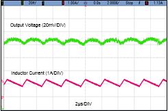
    1.     Device Images
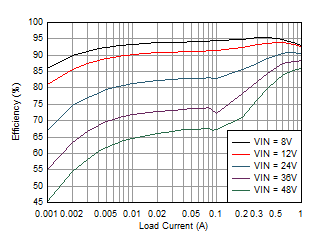
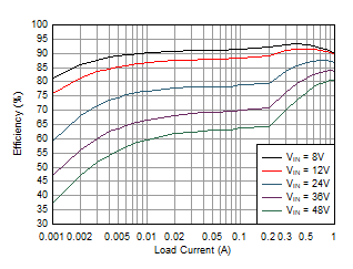
      1.      Efficiency versus Output Current VOUT = 5 V, 400 kHz
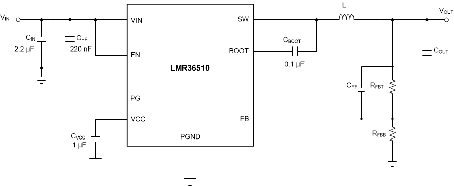
      2.      Simplified Schematic
  4. Revision History
  5. Pin Configuration and Functions
    1.     Pin Functions
  6. Specifications
    1. 6.1 Absolute Maximum Ratings
    2. 6.2 ESD Ratings
    3. 6.3 Recommended Operating Conditions
    4. 6.4 Thermal Information
    5. 6.5 Electrical Characteristics
    6. 6.6 Timing Requirements
    7. 6.7 Switching Characteristics
    8. 6.8 System Characteristics
    9. 6.9 Typical Characteristics
  7. Detailed Description
    1. 7.1 Overview
    2. 7.2 Functional Block Diagram
    3. 7.3 Feature Description
      1. 7.3.1 Power-Good Flag Output
      2. 7.3.2 Enable and Start-up
      3. 7.3.3 Current Limit and Short Circuit
      4. 7.3.4 Undervoltage Lockout and Thermal Shutdown
    4. 7.4 Device Functional Modes
      1. 7.4.1 Auto Mode
      2. 7.4.2 Dropout
      3. 7.4.3 Minimum Switch On-Time
  8. Application and Implementation
    1. 8.1 Application Information
    2. 8.2 Typical Application
      1. 8.2.1 Design 1: Low Power 24-V, 1-A Buck Converter
        1. 8.2.1.1 Design Requirements
        2. 8.2.1.2 Detailed Design Procedure
          1. 8.2.1.2.1  Choosing the Switching Frequency
          2. 8.2.1.2.2  Setting the Output Voltage
          3. 8.2.1.2.3  Inductor Selection
          4. 8.2.1.2.4  Output Capacitor Selection
          5. 8.2.1.2.5  Input Capacitor Selection
          6. 8.2.1.2.6  CBOOT
          7. 8.2.1.2.7  VCC
          8. 8.2.1.2.8  CFF Selection
          9. 8.2.1.2.9  External UVLO
          10. 8.2.1.2.10 Maximum Ambient Temperature
      2. 8.2.2 Application Curves
    3. 8.3 What to Do and What Not to Do
  9. Power Supply Recommendations
  10. 10Layout
    1. 10.1 Layout Guidelines
      1. 10.1.1 Ground and Thermal Considerations
    2. 10.2 Layout Example
  11. 11Device and Documentation Support
    1. 11.1 Device Support
      1. 11.1.1 Development Support
    2. 11.2 Documentation Support
      1. 11.2.1 Related Documentation
    3. 11.3 Receiving Notification of Documentation Updates
    4. 11.4 Support Resources
    5. 11.5 Trademarks
    6. 11.6 Electrostatic Discharge Caution
    7. 11.7 Glossary
  12. 12Mechanical, Packaging, and Orderable Information

Package Options

Mechanical Data (Package|Pins)
Thermal pad, mechanical data (Package|Pins)
Orderable Information

Application Curves

Unless otherwise specified, the following conditions apply: VIN = 24 V, TA = 25°C. Figure 34 shows the circuit with the appropriate BOM from Table 4.
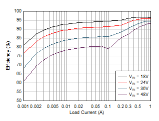
LMR36510 Efficiency_LMR36510_3p3V_22uH.gif
LMR36510A VOUT = 3.3 V 400 kHz
Figure 16. Efficiency
LMR36510 Efficiency_LMR36510_5V_22uH.gif
LMR36510A VOUT = 5 V 400 kHz
Figure 18. Efficiency
LMR36510 Efficiency_LMR36510_12V_47uH.gif
LMR36510A VOUT = 12 V 400 kHz
Figure 20. Efficiency
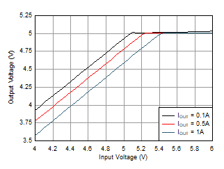
LMR36510 Dropout_LMR36510_5V_22uH.gif
LMR36510A VOUT = 5 V 400 kHz
Figure 22. Dropout Characteristic
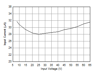
LMR36510 InputCurrentvsVin.gif
VOUT = 3.3 V IOUT = 0 A RFBT = 100 kΩ
RFBB = 43.2 kΩ
Figure 24. Input Supply Current
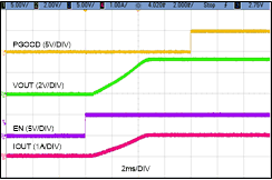
LMR36510 EN_Startup_Waveform.gif
VIN = 24 V VOUT = 3.3 V ILOAD = 1 A
Figure 26. Enable Start-Up Waveform
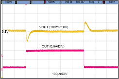
LMR36510 LoadTransient_24V_3p3VOUT_0p1_1A.gif
VOUT = 3.3 V 400 kHz ILOAD = 0.1 A - 1 A
Slew Rate = 1 A/µs
Figure 28. Load Transient
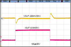
LMR36510 LoadTransient_24V_5VOUT_0p1_1A.gif
VOUT = 5 V 400 kHz ILOAD = 0.1 A -1 A
Slew Rate = 1 A/µs
Figure 30. Load Transient
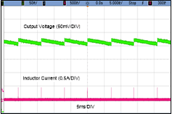
LMR36510 OutputRipple24V_5Vout_NL.gif
VIN = 24 V VOUT = 5 V ILOAD = 0 A
Figure 32. Output Ripple at No load
LMR36510 LoadRegulation_LMR36510_3p3V_22uH.gif
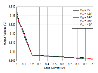
LMR36510A VOUT = 3.3 V 400 kHz
Figure 17. Load Regulation
LMR36510 LoadRegulation_LMR36510_5V_22uH.gif
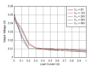
LMR36510A VOUT = 5 V 400 kHz
Figure 19. Load Regulation
LMR36510 LoadRegulation_LMR36510_12V_47uH.gif
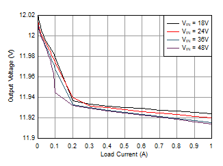
LMR36510A VOUT = 12 V 400 kHz
Figure 21. Load Regulation
LMR36510 Dropout_LMR36510_12V_47uH.gif
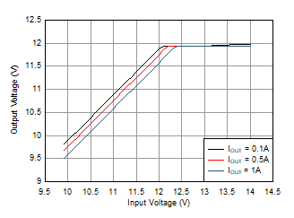
LMR36510A VOUT = 12 V 400 kHz
Figure 23. Dropout Characteristic
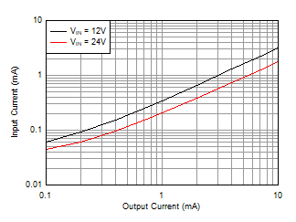
LMR36510 InputCurrentvsOutputCurrent.gif
VOUT = 3.3 V RFBT = 100 kΩ RFBB = 43.2 kΩ
Figure 25. Input Supply Current versus Load Current
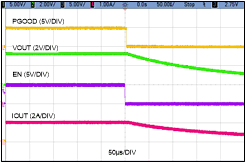
LMR36510 EN_Shutdown_Waveform.gif
VIN = 24 V VOUT = 3.3 V ILOAD = 1 A
Figure 27. Enable Shutdown Waveform
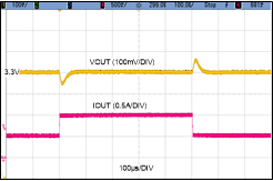
LMR36510 LoadTransient_24V_3p3VOUT_0p5_1A.gif
VOUT = 3.3 V 400 kHz ILOAD = 0.5 A - 1 A
Slew Rate = 1 A/µs
Figure 29. Load Transient
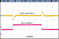
LMR36510 LoadTransient_24V_5VOUT_0p5_1A.gif
VOUT = 5 V 400 kHz ILOAD = 0.5 A -1 A
Slew Rate = 1 A/µs
Figure 31. Load Transient
LMR36510 OutputRipple24V_5Vout_1A.gif
VIN = 24 V VOUT = 5 V ILOAD = 1 A
Figure 33. Output Ripple at 1 A
LMR36510 Circuit_typical_apps_curve_10-ADJ-output.gifFigure 34. Circuit for Typical Application Curves

Table 4. BOM for Typical Application Curves

VOUT FREQUENCY L COUT RFBT RFBB CFF IC
3.3 V 400 kHz 22 µH, 99.65 mΩ 3 x 22 µF, 25V 46.4 kΩ 20.0 kΩ None LMR36510A
5 V 400 kHz 22 µH, 99.65 mΩ 2 x 22 µF, 25V 34.0 kΩ + 46.4 kΩ 20.0 kΩ None LMR36510A
12 V 400 kHz 47 µH, 100 mΩ 3 x 22 µF, 25V 100 kΩ 9.09 kΩ None LMR36510A