SNAS714C November   2016  – August 2021 LMS3635-Q1 , LMS3655-Q1

PRODUCTION DATA  

  1. Features
  2. Applications
  3. Description
  4. Revision History
  5. Device Comparison Tables
  6. Pin Configuration and Functions
  7. Specifications
    1. 7.1 Absolute Maximum Ratings
    2. 7.2 ESD Ratings
    3. 7.3 Recommended Operating Conditions
    4. 7.4 Thermal Information
    5. 7.5 Thermal Information (for Device Mounted on PCB)
    6. 7.6 Electrical Characteristics
    7. 7.7 System Characteristics
    8. 7.8 Timing Requirements
    9. 7.9 Typical Characteristics
  8. Detailed Description
    1. 8.1 Overview
    2. 8.2 Functional Block Diagram
      1. 8.2.1 Control Scheme
    3. 8.3 Feature Description
      1. 8.3.1 RESET Flag Output
      2. 8.3.2 Enable and Start-Up
      3. 8.3.3 Soft-Start Function
      4. 8.3.4 Current Limit
      5. 8.3.5 Hiccup Mode
      6. 8.3.6 Synchronizing Input
      7. 8.3.7 Undervoltage Lockout (UVLO) and Thermal Shutdown (TSD)
      8. 8.3.8 Input Supply Current
    4. 8.4 Device Functional Modes
      1. 8.4.1 AUTO Mode
      2. 8.4.2 FPWM Mode
      3. 8.4.3 Dropout
      4. 8.4.4 Spread-Spectrum Operation
  9. Application and Implementation
    1. 9.1 Application Information
    2. 9.2 Typical Applications
      1. 9.2.1 General Application
        1. 9.2.1.1 Design Requirements
        2. 9.2.1.2 Detailed Design Procedure
          1. 9.2.1.2.1 Custom Design With WEBENCH® Tools
          2. 9.2.1.2.2 External Components Selection
            1. 9.2.1.2.2.1 Input Capacitors
            2. 9.2.1.2.2.2 Output Inductors and Capacitors
              1. 9.2.1.2.2.2.1 Inductor Selection
              2. 9.2.1.2.2.2.2 Output Capacitor Selection
          3. 9.2.1.2.3 Setting the Output Voltage
          4. 9.2.1.2.4 FB for Adjustable Output
          5. 9.2.1.2.5 VCC
          6. 9.2.1.2.6 BIAS
          7. 9.2.1.2.7 CBOOT
          8. 9.2.1.2.8 Maximum Ambient Temperature
        3. 9.2.1.3 Application Curves
      2. 9.2.2 Fixed 5-V Output for USB-Type Applications
        1. 9.2.2.1 Design Requirements
        2. 9.2.2.2 Detailed Design Procedure
        3. 9.2.2.3 Application Curves
      3. 9.2.3 Fixed 3.3-V Output
        1. 9.2.3.1 Design Requirements
        2. 9.2.3.2 Detailed Design Procedure
        3. 9.2.3.3 Application Curves
      4. 9.2.4 6-V Adjustable Output
        1. 9.2.4.1 Design Requirements
        2. 9.2.4.2 Detailed Design Procedure
        3. 9.2.4.3 Application Curves
    3. 9.3 Do's and Don't's
  10. 10Power Supply Recommendations
  11. 11Layout
    1. 11.1 Layout Guidelines
    2. 11.2 Layout Example
  12. 12Device and Documentation Support
    1. 12.1 Device Support
      1. 12.1.1 Third-Party Products Disclaimer
      2. 12.1.2 Development Support
        1. 12.1.2.1 Custom Design With WEBENCH® Tools
    2. 12.2 Documentation Support
      1. 12.2.1 Related Documentation
    3. 12.3 Receiving Notification of Documentation Updates
    4. 12.4 Support Resources
    5. 12.5 Trademarks
    6. 12.6 Electrostatic Discharge Caution
    7. 12.7 Glossary
  13. 13Mechanical, Packaging, and Orderable Information

Package Options

Mechanical Data (Package|Pins)
Thermal pad, mechanical data (Package|Pins)
Orderable Information

Enable and Start-Up

Start-up and shutdown of the LMS36x5-Q1 are controlled by the EN input. Applying a voltage of ≥ 2 V activates the device, while a voltage of ≤ 1.45 V is required for shutdown. The EN input may also be connected directly to the input voltage supply. This input must not be left floating. The LMS36x5-Q1 uses a reference-based soft start that prevents output voltage overshoots and large inrush currents as the regulator is starting up.

A typical start-up waveform is shown in Figure 8-4 along with timing definitions. This waveform indicates the sequence and timing between the enable input, output voltage, and RESET. From the figure, the user can define several different start-up times depending on what is relevant to the application. Table 8-1 lists the timing definitions and typical values.
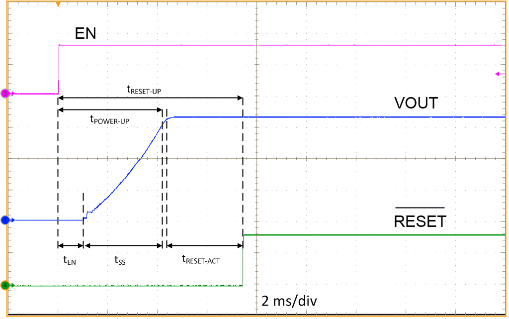
GUID-BB055A89-92AA-4CE1-AB0F-C25526142EBB-low.gifFigure 8-4 Typical Start-Up Waveform
Table 8-1 Typical Start-Up Times
PARAMETERDEFINITIONVALUEUNIT
tRESET-READYTotal start-up sequence timeTime from EN to RESET released7.5ms
tPOWER-UPStart-up timeTime from EN to 90% of VOUT4ms
tSSSoft-start timeRise time of VOUT from 10% to 90%3.2ms
tENDelay timeTime from EN to start of VOUT rising1ms
tRESET-ACTRESET timeTime from output voltage within 94% and RESET released3ms