SLOS447J September 2004 – June 2025 LMV341 , LMV342 , LMV344
PRODUCTION DATA
- 1
- 1 Features
- 2 Applications
- 3 Description
- 4 Pin Configuration and Functions
- 5 Specifications
- 6 Detailed Description
- 7 Application and Implementation
- 8 Power Supply Recommendations
- 9 Layout
- 10Device and Documentation Support
- 11Revision History
- 12Mechanical, Packaging, and Orderable Information
Package Options
Refer to the PDF data sheet for device specific package drawings
Mechanical Data (Package|Pins)
- D|8
- DGK|8
Thermal pad, mechanical data (Package|Pins)
Orderable Information
3 Description
The LMV34x devices are single, dual,
and quad CMOS operational amplifiers, respectively, with low voltage, low power, and
rail-to-rail output swing capabilities. The PMOS input stage offers an ultra-low
input bias current of 1pA (typical) and an offset voltage of 0.25mV (typical). The
single-supply amplifier is designed specifically for low-voltage
(2.7V to 5V) operation, with a wide common-mode input
voltage range that typically extends from –0.2V to 0.8V from the positive supply
rail. The LMV341 (single) also offers a shutdown ( SHDN) pin
that can be used to disable the device. In shutdown mode, the supply current is
reduced to 33nA (typical). Additional features of the family are a 20nV/√
Hz voltage noise at 10kHz, 1MHz unity-gain bandwidth, 1V/μs
slew rate, and 100μA current consumption per channel.
Offered in both the SOT-23 and smaller SC70 packages, the LMV341 is suitable for the most space-constraint applications. The LMV342 dual device is offered in the standard SOIC and VSSOP packages. An extended industrial temperature range from –40°C to 125°C makes these devices suitable in a wide variety of commercial and industrial environments.
| PART NUMBER(1) | PACKAGE | BODY SIZE (NOM) |
|---|---|---|
| LMV341IDCK | DCK (SC70, 6) | 2.00mm × 1.25mm |
| LMV341IDBV | DBV (SOT-23, 6) | 2.90mm ×1.60mm |
| LMV342ID | D (SOIC, 8) | 4.90mm × 3.91mm |
| LMV342IDGK | DGK (VSSOP, 8) | 3.00mm × 3.00mm |
| LMV344ID | D (SOIC, 14) | 8.65mm × 3.91mm |
| LMV344IPW | PW (TSSOP, 14) | 5.00mm × 4.40mm |
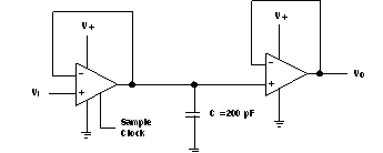
 Sample-and-Hold
Circuit