SNOSAZ6C August 2008 – November 2015 LMV831 , LMV832 , LMV834
PRODUCTION DATA.
- 1 Features
- 2 Applications
- 3 Description
- 4 Revision History
- 5 Pin Configuration and Functions
- 6 Specifications
- 7 Detailed Description
- 8 Application and Implementation
- 9 Power Supply Recommendations
- 10Layout
- 11Device and Documentation Support
- 12Mechanical, Packaging, and Orderable Information
Package Options
Mechanical Data (Package|Pins)
- DGK|8
Thermal pad, mechanical data (Package|Pins)
- DGK|8
Orderable Information
7.4.2 CMRR Measurement
The CMRR measurement results may need some clarification. This is because different set-ups are used to measure the AC CMRR and the DC CMRR.
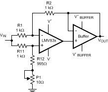
The DC CMRR is derived from ΔVOS versus ΔVCM. This value is stated in the tables, and is tested during production testing. The AC CMRR is measured with the test circuit shown in Figure 47.
 Figure 47. AC CMRR Measurement Set-Up
The configuration is largely the usually applied balanced configuration. With potentiometer P1, the balance can be tuned to compensate for the DC offset in the DUT. The main difference is the addition of the buffer. This buffer prevents the open-loop output impedance of the DUT from affecting the balance of the feedback network. Now the closed-loop output impedance of the buffer is a part of the balance. As the closed-loop output impedance is much lower, and by careful selection of the buffer also has a larger bandwidth, the total effect is that the CMRR of the DUT can be measured much more accurately. The differences are apparent in the larger measured bandwidth of the AC CMRR.
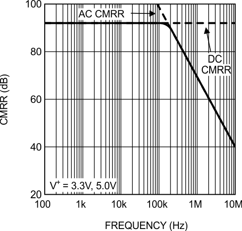
One artifact from this test circuit is that the low frequency CMRR results appear higher than expected. This is because in the AC CMRR test circuit the potentiometer is used to compensate for the DC mismatches. So, mainly AC mismatch is all that remains. Therefore, the obtained DC CMRR from this AC CMRR test circuit tends to be higher than the actual DC CMRR based on DC measurements.
The CMRR curve in Figure 48 shows a combination of the AC CMRR and the DC CMRR.
 Figure 48. CMRR Curve