SNVS641L January 2010 – April 2019 LMZ10503
PRODUCTION DATA.
- 1 Features
- 2 Applications
- 3 Description
- 4 Revision History
- 5 Pin Configuration and Functions
- 6 Specifications
- 7 Detailed Description
- 8 Application and Implementation
- 9 Power Supply Recommendations
- 10Layout
- 11Device and Documentation Support
- 12Mechanical, Packaging, and Orderable Information
Package Options
Mechanical Data (Package|Pins)
- NDW|7
Thermal pad, mechanical data (Package|Pins)
Orderable Information
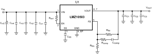
8.3.2 Application Schematic for 3.3-V to 5-V Input and 2.5-V Output
The compensation for each solution was optimized to work over the full input range. Many applications have a fixed input voltage rail. It is possible to modify the compensation to obtain a faster transient response for a given input voltage operating point.
 Figure 27. Schematic for 2.5-V Output Based on 3.3-V to 5-V Input
 Table 7. Bill of Materials for Evaluation Board, VIN = 3.3 V to 5 V, VOUT = 2.5 V, IOUT (MAX) = 3 A
| DESIGNATOR | DESCRIPTION | CASE SIZE | MANUFACTURER | MANUFACTURER P/N | QUANTITY |
|---|---|---|---|---|---|
| U1 | Power Module | PFM-7 | Texas Instruments | LMZ10503 | 1 |
| Cin1 | 1 µF, X7R, 16 V | 0805 | TDK | C2012X7R1C105K | 1 |
| Cin2, CO1 | 4.7 µF, X5R, 6.3 V | 0805 | TDK | C2012X5R0J475K | 2 |
| Cin3, CO2 | 22 µF, X5R, 16 V | 1210 | TDK | C3225X5R1C226M | 2 |
| Cin4 | 47 µF, X5R, 6.3 V | 1210 | TDK | C3225X5R0J476M | 1 |
| Cin5 | 220 µF, 10 V, AL-Elec | E | Panasonic | EEE1AA221AP | 1 |
| CO3 | 100 µF, X5R, 6.3 V | 1812 | TDK | C4532X5R0J107M | 1 |
| Rfbt | 75 kΩ | 0805 | Vishay Dale | CRCW080575K0FKEA | 1 |
| Rfbb | 34.8 kΩ | 0805 | Vishay Dale | CRCW080534K8FKEA | 1 |
| Rcomp | 1.1 kΩ | 0805 | Vishay Dale | CRCW08051K10FKEA | 1 |
| Ccomp | 180 pF, ±5%, C0G, 50 V | 0603 | TDK | C1608C0G1H181J | 1 |
| Ren1 | 100 kΩ | 0805 | Vishay Dale | CRCW0805100KFKEA | 1 |
| CSS | 10 nF, ±5%, C0G, 50 V | 0805 | TDK | C2012C0G1H103J | 1 |
Table 8. Output Voltage Setting (Rfbt = 75 kΩ)
| VOUT | Rfbb | |||
|---|---|---|---|---|
| 3.3V | 23.7 kΩ | |||
| 2.5 V | 34.8 kΩ | |||
| 1.8 V | 59 kΩ | |||
| 1.5 V | 84.5 kΩ | |||
| 1.2 V | 150 kΩ | |||
| 0.9 V | 590 kΩ | |||