SNVS665H June 2010 – October 2015 LMZ14202EXT
PRODUCTION DATA.
- 1 Features
- 2 Applications
- 3 Description
- 4 Revision History
- 5 Pin Configuration and Functions
- 6 Specifications
- 7 Detailed Description
- 8 Application and Implementation
- 9 Power Supply Recommendations
- 10Layout
- 11Device and Documentation Support
- 12Mechanical, Packaging, and Orderable Information
Package Options
Mechanical Data (Package|Pins)
- NDW|7
Thermal pad, mechanical data (Package|Pins)
Orderable Information
6 Specifications
6.1 Absolute Maximum Ratings
over operating free-air temperature range (unless otherwise noted)(1)(2)| MIN | MAX | UNIT | |
|---|---|---|---|
| VIN, RON to GND | –0.3 | 43.5 | V |
| EN, FB, SS to GND | –0.3 | 7 | V |
| Junction temperature | 150 | °C | |
| Peak reflow case temperature (30 sec) | 245 | °C | |
| Storage temperature | –65 | 150 | °C |
(1) Stresses beyond those listed under Absolute Maximum Ratings may cause permanent damage to the device. These are stress ratings only, which do not imply functional operation of the device at these or any other conditions beyond those indicated under Recommended Operating Conditions. Exposure to absolute-maximum-rated conditions for extended periods may affect device reliability.
(2) For soldering specifications, refer to Absolute Maximum Ratings for Soldering SNOA549.
6.2 ESD Ratings
| VALUE | UNIT | |||
|---|---|---|---|---|
| V(ESD) | Electrostatic discharge | Human body model (HBM), per ANSI/ESDA/JEDEC JS-001(1)(2) | ±2000 | V |
(1) JEDEC document JEP155 states that 500-V HBM allows safe manufacturing with a standard ESD control process.
(2) The human body model is a 100-pF capacitor discharged through a 1.5-kΩ resistor into each pin. Test method is per JESD-22-114.
6.3 Recommended Operating Conditions
over operating free-air temperature range (unless otherwise noted)| MIN | MAX | UNIT | |
|---|---|---|---|
| VIN | 6 | 42 | V |
| EN | 0 | 6.5 | V |
| Operation Junction Temperature | −55 | 125 | °C |
6.4 Thermal Information
| THERMAL METRIC(1) | LMZ14202EXT | UNIT | ||
|---|---|---|---|---|
| NDW (TO-PMOD) | ||||
| 7 PINS | ||||
| RθJA | Junction-to-ambient thermal resistance(2) | 4-layer JEDEC Printed-Circuit-Board, 100 vias, No air flow | 19.3 | °C/W |
| 2-layer JEDEC Printed-Circuit-Board, No air flow | 21.5 | |||
| RθJC(top) | Junction-to-case (top) thermal resistance | No air flow | 1.9 | °C/W |
(1) For more information about traditional and new thermal metrics, see the Semiconductor and IC Package Thermal Metrics application report, SPRA953.
(2) RθJA measured on a 1.705-in × 3.0-in 4-layer board, with 1-oz copper, thirty five thermal vias, no air flow, and 1-W power dissipation. Refer to Figure 41.
6.5 Electrical Characteristics
Limits in standard type are for TJ = 25°C, unless otherwise specified. Minimum and Maximum limits are ensured through test, design or statistical correlation. Typical values represent the most likely parametric norm at TJ = 25°C, and are provided for reference purposes only. Unless otherwise stated the following conditions apply: VIN = 24 V, VOUT = 3.3 V.| PARAMETER | TEST CONDITIONS | MIN(1) | TYP(2) | MAX(1) | UNIT | ||
|---|---|---|---|---|---|---|---|
| SYSTEM PARAMETERS | |||||||
| ENABLE CONTROL(3) | |||||||
| VEN | EN threshold trip point | VEN rising | 1.18 | V | |||
| over the junction temperature (TJ) range of –55°C to +125°C | 1.1 | 1.26 | |||||
| VEN-HYS | EN threshold hysteresis | VEN falling | 90 | mV | |||
| SOFT-START | |||||||
| ISS | SS source current | VSS = 0 V | 8 | µA | |||
| over the junction temperature (TJ) range of –55°C to +125°C | 4.9 | 11 | |||||
| ISS-DIS | SS discharge current | –200 | µA | ||||
| CURRENT LIMIT | |||||||
| ICL | Current limit threshold | DC average | 2.6 | A | |||
| over the junction temperature (TJ) range of –55°C to +125°C | 2.3 | 3.65 | |||||
| REGULATION AND OVERVOLTAGE COMPARATOR | |||||||
| VFB | In-regulation feedback voltage | VSS >+ 0.8 V TJ = –55°C to 125°C IO = 2 A |
0.795 | V | |||
| over the junction temperature (TJ) range of –55°C to +125°C | 0.775 | 0.815 | |||||
| VSS >+ 0.8 V TJ = 25°C IO = 10 mA |
0.786 | 0.802 | 0.818 | V | |||
| VFB-OV | Feedback overvoltage protection threshold | 0.92 | V | ||||
| IFB | Feedback input bias current | 5 | nA | ||||
| IQ | Non-switching input current | VFB = 0.86 V | 1 | mA | |||
| ISD | Shutdown quiescent current | VEN = 0 V | 25 | μA | |||
| THERMAL CHARACTERISTICS | |||||||
| TSD | Thermal shutdown | Rising | 165 | °C | |||
| TSD-HYST | Thermal shutdown hysteresis | Falling | 15 | °C | |||
| PERFORMANCE PARAMETERS | |||||||
| ΔVO | Output voltage ripple | 8 | mVPP | ||||
| ΔVO/ΔVIN | Line regulation | VIN = 12 V to 42 V, IO = 2 A | 0.01% | ||||
| ΔVO/IOUT | Load regulation | VIN = 24 V | 1.5 | mV/A | |||
| η | Efficiency | VIN = 24 V, VO = 3.3 V, IO = 1 A | 86% | ||||
| VIN = 24 V, VO = 3.3 V, IO = 2 A | 85% | ||||||
(1) Minimum and Maximum limits are 100% production tested at 25°C. Limits over the operating temperature range are ensured through correlation using Statistical Quality Control (SQC) methods. Limits are used to calculate Average Outgoing Quality Level (AOQL).
(2) Typical numbers are at 25°C and represent the most likely parametric norm.
(3) EN 55022:2006, +A1:2007, FCC Part 15 Subpart B: 2007. See AN-2024 SNVA422 and layout for information on device under test.
6.6 Switching Characteristics
over operating free-air temperature range (unless otherwise noted)| PARAMETER | TEST CONDITIONS | MIN | TYP | MAX | UNIT | |
|---|---|---|---|---|---|---|
| ON/OFF TIMER | ||||||
| tON-MIN | ON timer minimum pulse width | 150 | ns | |||
| tOFF | OFF timer pulse width | 260 | ns | |||
6.7 Typical Characteristics
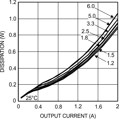
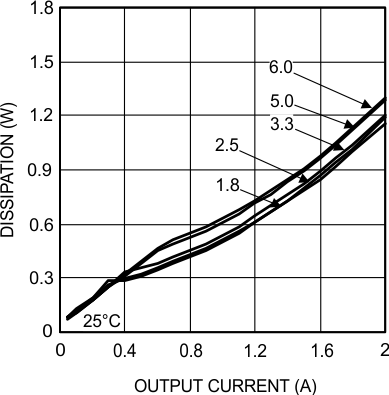
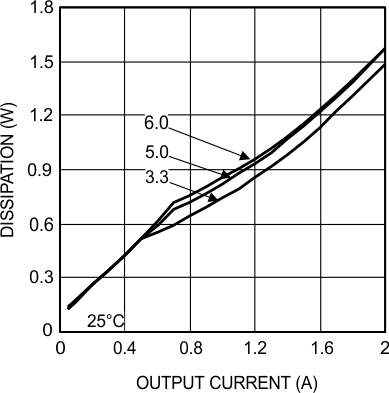
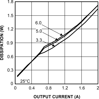
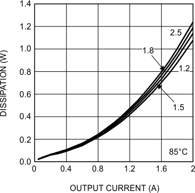
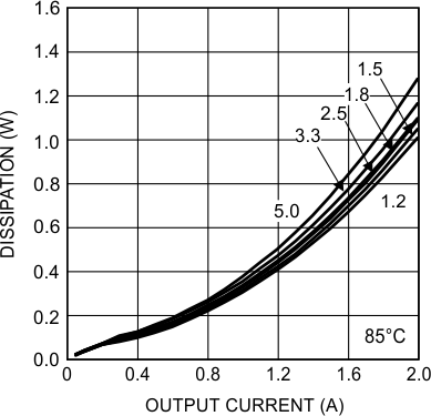
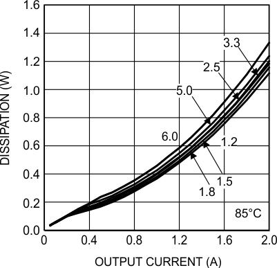
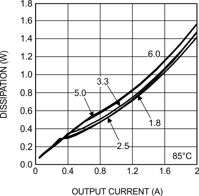
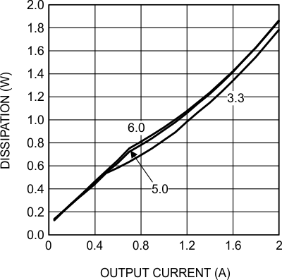
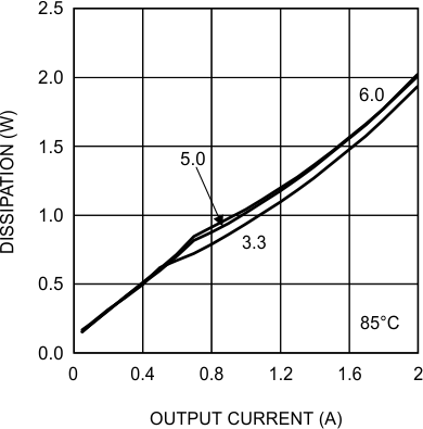
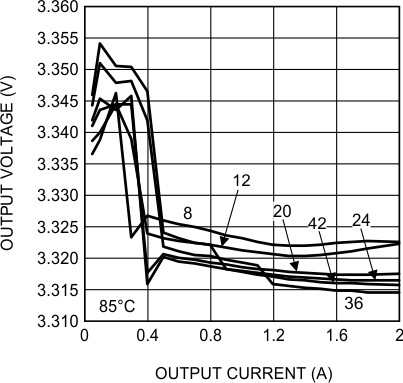
Unless otherwise specified, the following conditions apply: VIN = 24 V; CIN = 10-µF X7R Ceramic; CO = 100-µF X7R Ceramic; TA = 25°C for efficiency curves and waveforms.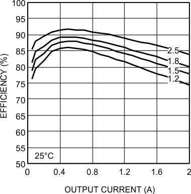
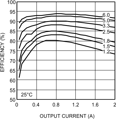
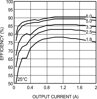
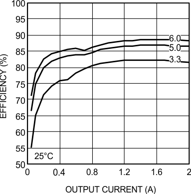
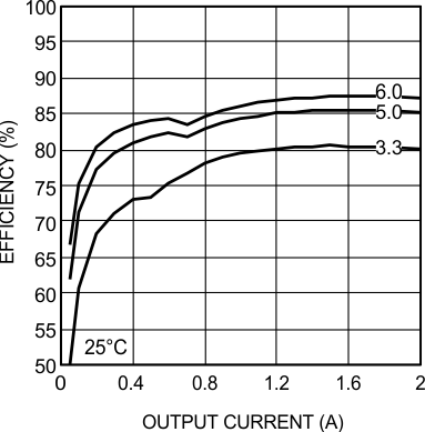
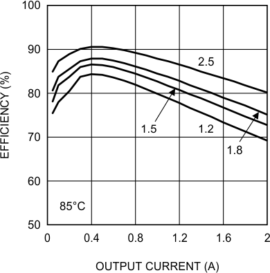
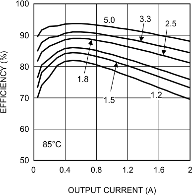
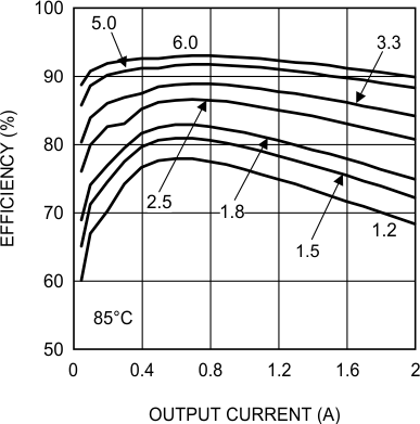
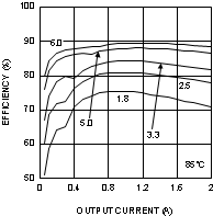
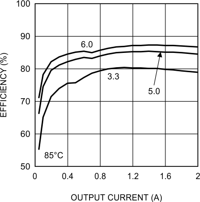
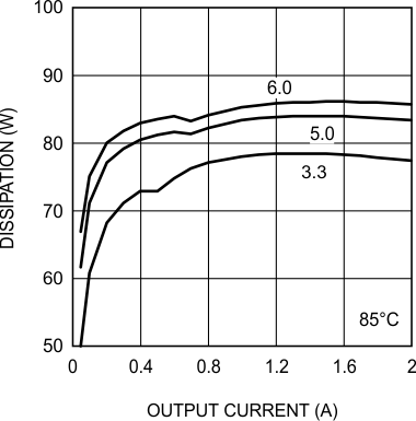
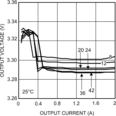
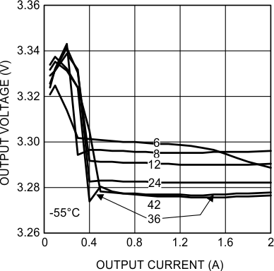
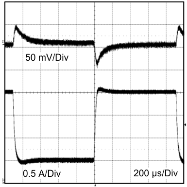
24-VIN 3.3-VO 0.6-A to 2-A Step
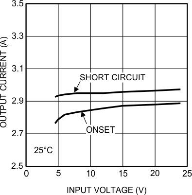
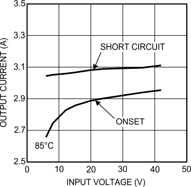
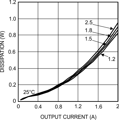
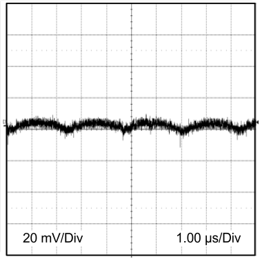
24-VIN 3.3-VO 2A, BW = 200 MHz
