SNVS691H January 2011 – October 2015 LMZ14202H
PRODUCTION DATA.
- 1 Features
- 2 Applications
- 3 Description
- 4 Revision History
- 5 Pin Configuration and Functions
- 6 Specifications
- 7 Detailed Description
-
8 Application and Implementation
- 8.1 Application Information
- 8.2
Typical Application
- 8.2.1 Design Requirements
- 8.2.2
Detailed Design Procedure
- 8.2.2.1 Design Steps for the LMZ14202H Application
- 8.2.3 Application Curves
- 9 Power Supply Recommendations
- 10Layout
- 11Device and Documentation Support
- 12Mechanical, Packaging, and Orderable Information
Package Options
Mechanical Data (Package|Pins)
- NDW|7
Thermal pad, mechanical data (Package|Pins)
Orderable Information
7 Detailed Description
7.1 Overview
7.1.1 COT Control Circuit Overview
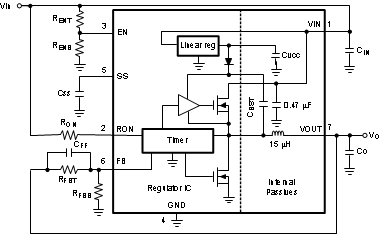
Constant On Time control is based on a comparator and an ON-time one-shot, with the output voltage feedback compared to an internal 0.8-V reference. If the feedback voltage is below the reference, the high-side MOSFET is turned on for a fixed ON-time determined by a programming resistor RON. RON is connected to VIN such that ON-time is reduced with increasing input supply voltage. Following this ON-time, the high-side MOSFET remains off for a minimum of 260 ns. If the voltage on the feedback pin falls below the reference level again the ON-time cycle is repeated. Regulation is achieved in this manner.
7.2 Functional Block Diagram

7.3 Feature Description
7.3.1 Output Overvoltage Comparator
The voltage at FB is compared to a 0.92-V internal reference. If FB rises above 0.92 V the ON-time is immediately terminated. This condition is known as overvoltage protection (OVP). It can occur if the input voltage is increased very suddenly or if the output load is decreased very suddenly. Once OVP is activated, the top MOSFET ON-times will be inhibited until the condition clears. Additionally, the synchronous MOSFET will remain on until inductor current falls to zero.
7.3.2 Current Limit
Current limit detection is carried out during the OFF-time by monitoring the current in the synchronous MOSFET. Referring to the Functional Block Diagram, when the top MOSFET is turned off, the inductor current flows through the load, the PGND pin and the internal synchronous MOSFET. If this current exceeds ICL the current limit comparator disables the start of the next ON-time period. The next switching cycle will occur only if the FB input is less than 0.8 V and the inductor current has decreased below ICL. Inductor current is monitored during the period of time the synchronous MOSFET is conducting. So long as inductor current exceeds ICL, further ON-time intervals for the top MOSFET will not occur. Switching frequency is lower during current limit due to the longer OFF-time.
NOTE
The DC current limit varies with duty cycle, switching frequency, and temperature.
7.3.3 Thermal Protection
The junction temperature of the LMZ14202H should not be allowed to exceed its maximum ratings. Thermal protection is implemented by an internal Thermal Shutdown circuit which activates at 165 °C (typical) causing the device to enter a low power standby state. In this state the main MOSFET remains off causing VO to fall, and additionally the CSS capacitor is discharged to ground. Thermal protection helps prevent catastrophic failures for accidental device overheating. When the junction temperature falls back below 145 °C (typical Hyst = 20 °C) the SS pin is released, VO rises smoothly, and normal operation resumes.
7.3.4 Zero Coil Current Detection
The current of the lower (synchronous) MOSFET is monitored by a zero coil current detection circuit which inhibits the synchronous MOSFET when its current reaches zero until the next ON-time. This circuit enables the DCM operating mode, which improves efficiency at light loads.
7.3.5 Prebiased Start-Up
The LMZ14202H will properly start up into a prebiased output. This is start-up situation is common in multiple rail logic applications where current paths may exist between different power rails during the start-up sequence. The pre-bias level of the output voltage must be less than the input UVLO set point. This will prevent the output prebias from enabling the regulator through the high-side MOSFET body diode.
7.4 Device Functional Modes
7.4.1 Discontinuous Conduction and Continuous Conduction Modes
At light load the regulator will operate in discontinuous conduction mode (DCM). With load currents above the critical conduction point, it will operate in continuous conduction mode (CCM). When operating in DCM the switching cycle begins at zero amps inductor current; increases up to a peak value, and then recedes back to zero before the end of the OFF-time. During the period of time that inductor current is zero, all load current is supplied by the output capacitor. The next ON-time period starts when the voltage on the FB pin falls below the internal reference. The switching frequency is lower in DCM and varies more with load current as compared to CCM. Conversion efficiency in DCM is maintained because conduction and switching losses are reduced with the smaller load and lower switching frequency.