SNVS691H January 2011 – October 2015 LMZ14202H
PRODUCTION DATA.
- 1 Features
- 2 Applications
- 3 Description
- 4 Revision History
- 5 Pin Configuration and Functions
- 6 Specifications
- 7 Detailed Description
-
8 Application and Implementation
- 8.1 Application Information
- 8.2
Typical Application
- 8.2.1 Design Requirements
- 8.2.2
Detailed Design Procedure
- 8.2.2.1 Design Steps for the LMZ14202H Application
- 8.2.3 Application Curves
- 9 Power Supply Recommendations
- 10Layout
- 11Device and Documentation Support
- 12Mechanical, Packaging, and Orderable Information
Package Options
Mechanical Data (Package|Pins)
- NDW|7
Thermal pad, mechanical data (Package|Pins)
Orderable Information
10 Layout
10.1 Layout Guidelines
PCB layout is an important part of DC-DC converter design. Poor board layout can disrupt the performance of a DC-DC converter and surrounding circuitry by contributing to EMI, ground bounce and resistive voltage drop in the traces. These can send erroneous signals to the DC-DC converter resulting in poor regulation or instability. Good layout can be implemented by following a few simple design rules.
- Minimize area of switched current loops.
- Have a single point ground.
- Minimize trace length to the FB pin.
- Make input and output bus connections as wide as possible.
- Provide adequate device heat-sinking.
From an EMI reduction standpoint, it is imperative to minimize the high di/dt paths during PC board layout. The high current loops that do not overlap have high di/dt content that will cause observable high frequency noise on the output pin if the input capacitor (Cin1) is placed at a distance away from the LMZ14202H. Therefore place CIN1 as close as possible to the LMZ14202H VIN and GND exposed pad. This will minimize the high di/dt area and reduce radiated EMI. Additionally, grounding for both the input and output capacitor should consist of a localized top side plane that connects to the GND exposed pad (EP).
The ground connections for the feedback, soft-start, and enable components should be routed to the GND pin of the device. This prevents any switched or load currents from flowing in the analog ground traces. If not properly handled, poor grounding can result in degraded load regulation or erratic output voltage ripple behavior. Provide the single point ground connection from pin 4 to EP.
Both feedback resistors, RFBT and RFBB, and the feed forward capacitor CFF, should be close to the FB pin. Because the FB node is high impedance, maintain the copper area as small as possible. The traces from RFBT, RFBB, and CFF should be routed away from the body of the LMZ14202H to minimize noise pickup.
This reduces any voltage drops on the input or output of the converter and maximizes efficiency. To optimize voltage accuracy at the load, ensure that a separate feedback voltage sense trace is made to the load. Doing so will correct for voltage drops and provide optimum output accuracy.
Use an array of heat-sinking vias to connect the exposed pad to the ground plane on the bottom PCB layer. If the PCB has a plurality of copper layers, these thermal vias can also be employed to make connection to inner layer heat-spreading ground planes. For best results use a 6 × 6 via array with minimum via diameter of 8 mils thermal vias spaced 59 mils (1.5 mm). Ensure enough copper area is used for heat-sinking to keep the junction temperature below 125°C.
10.1.1 Power Module SMT Guidelines
The recommendations below are for a standard module surface mount assembly
- Land Pattern – Follow the PCB land pattern with either soldermask defined or non-soldermask defined pads
- Stencil Aperture
- For the exposed die attach pad (DAP), adjust the stencil for approximately 80% coverage of the PCB land pattern
- For all other I/O pads use a 1:1 ratio between the aperture and the land pattern recommendation
- Solder Paste – Use a standard SAC Alloy such as SAC 305, type 3 or higher
- Stencil Thickness – 0.125 mm to 0.15 mm
- Reflow - Refer to solder paste supplier recommendation and optimized per board size and density
- Refer to application note SNAA214 for Reflow information
- Maximum number of reflows allowed is one
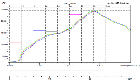 Figure 50. Sample Reflow Profile
Table 1. Sample Reflow Profile Table
| PROBE | MAX TEMP (°C) | REACHED MAX TEMP | TIME ABOVE 235°C | REACHED 235°C | TIME ABOVE 245°C | REACHED 245°C | TIME ABOVE 260°C | REACHED 260°C |
|---|---|---|---|---|---|---|---|---|
| 1 | 242.5 | 6.58 | 0.49 | 6.39 | 0.00 | – | 0.00 | – |
| 2 | 242.5 | 7.10 | 0.55 | 6.31 | 0.00 | 7.10 | 0.00 | – |
| 3 | 241.0 | 7.09 | 0.42 | 6.44 | 0.00 | – | 0.00 | – |
10.2 Layout Example
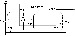 Figure 51. Critical Current Loops to Minimize
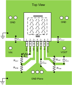 Figure 52. PCB Layout
10.3 Power Dissipation and Board Thermal Requirements
For a design case of VIN = 24 V, VOUT = 12 V, IOUT = 2 A, TA (MAX) = 85°C , and TJUNCTION = 125°C, the device must see a maximum junction-to-ambient thermal resistance of:
RθJA-MAX < (TJ-MAX - TA(MAX)) / PD
This RθJA-MAX will ensure that the junction temperature of the regulator does not exceed TJ-MAX in the particular application ambient temperature.
To calculate the required RθJA-MAX we need to get an estimate for the power losses in the IC. Figure 53 is taken from the Typical Characteristics section and shows the power dissipation of the LMZ14202H for VOUT = 12 V at 85°C TA.
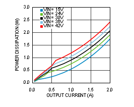 Figure 53. Power Dissipation VOUT = 12 V, TA = 85°C
Using the 85°C TA power dissipation data PD for VIN = 24 V and VOUT = 12 V is estimated to be 1.8 W. The necessary RθJA-MAX can now be calculated.
To achieve this thermal resistance the PCB is required to dissipate the heat effectively. The area of the PCB will have a direct effect on the overall junction-to-ambient thermal resistance. In order to estimate the necessary copper area we can refer to the following Figure 54. Figure 54 is taken from the Typical Characteristics section and shows how the RθJA varies with the PCB area.
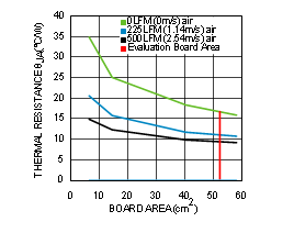 Figure 54. Package Thermal Resistance RθJA 4-Layer Printed-Circuit-Board With 1-oz Copper
For RθJA-MAX< 22.2°C/W and only natural convection (that is, no air flow), the PCB area will have to be at least 30 cm2. This corresponds to a square board with approximately 5.5cm × 5.5cm (2.17in × 2.17in) copper area, 4 layers, and 1-oz copper thickness. Higher copper thickness will further improve the overall thermal performance. Note that thermal vias should be placed under the IC package to easily transfer heat from the top layer of the PCB to the inner layers and the bottom layer.
For more guidelines and insight on PCB copper area, thermal vias placement, and general thermal design practices refer to Application Note AN-2020 (SNVA419).