SNVS874E August 2012 – September 2021 LMZ20501
PRODUCTION DATA
- 1 Features
- 2 Applications
- 3 Description
- 4 Revision History
- 5 Pin Configuration and Functions
- 6 Specifications
- 7 Detailed Description
- 8 Application and Implementation
- 9 Power Supply Recommendations
- 10Layout
- 11Device and Documentation Support
- 12Mechanical, Packaging, and Orderable Information
Package Options
Refer to the PDF data sheet for device specific package drawings
Mechanical Data (Package|Pins)
- SIL|8
Thermal pad, mechanical data (Package|Pins)
Orderable Information
10.1 Layout Guidelines
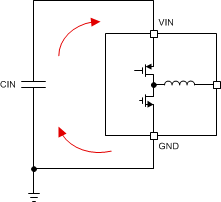
The PCB layout of any DC-DC converter is critical to the optimal performance of the design. Bad PCB layout can disrupt the operation of an otherwise good schematic design. Even if the converter regulates correctly, bad PCB layout can mean the difference between a robust design and one that cannot be mass produced. Furthermore, the EMI performance of the regulator is dependent on the PCB layout, to a great extent. In a buck converter, the most critical PCB feature is the loop formed by the input capacitor and the module ground, as shown in Figure 10-1. This loop carries fast transient currents that can cause large transient voltages when reacting with the trace inductance. These unwanted transient voltages will disrupt the proper operation of the converter. Because of this, the traces in this loop should be wide and short, and the loop area as small as possible to reduce the parasitic inductance. Figure 10-2 shows a recommended layout for the critical components of the LMZ20501; the top side metal is shown in red. This PCB layout is a good guide for any specific application. The following important guidelines should also be followed:
- Place the input capacitor CIN as close as possible to the VIN and GND terminals. VIN (pin 8) and GND (pin 6) are on the same side of the module, simplifying the input capacitor placement.
- Place the feedback divider as close as possible to the FB pin on the module. The divider and CFF should be close to the module, while the length of the trace from VOUT to the divider can be somewhat longer. However, this latter trace should not be routed near any noise sources that can capacitively couple to the FB input.
- Connect the EP pad to the GND plane. This pad acts as a heat-sink connection and a ground connection for the module. It must be solidly connected to a ground plane. The integrity of this connection has a direct bearing on the effective RθJA.
- Provide enough PCB area for proper heat-sinking. As stated in Section 8.2.1.5, enough copper area must be used to provide a low RθJA, commensurate with the maximum load current and ambient temperature. The top and bottom PCB layers should be made with two ounce copper; and no less than one ounce.
- The resources in Table 11-2 provide additional important guidelines.
 Figure 10-1 Current Loops With Fast Transient Currents