SNVS874E August 2012 – September 2021 LMZ20501
PRODUCTION DATA
- 1 Features
- 2 Applications
- 3 Description
- 4 Revision History
- 5 Pin Configuration and Functions
- 6 Specifications
- 7 Detailed Description
- 8 Application and Implementation
- 9 Power Supply Recommendations
- 10Layout
- 11Device and Documentation Support
- 12Mechanical, Packaging, and Orderable Information
Package Options
Refer to the PDF data sheet for device specific package drawings
Mechanical Data (Package|Pins)
- SIL|8
Thermal pad, mechanical data (Package|Pins)
Orderable Information
7.3.5 Dropout Behavior
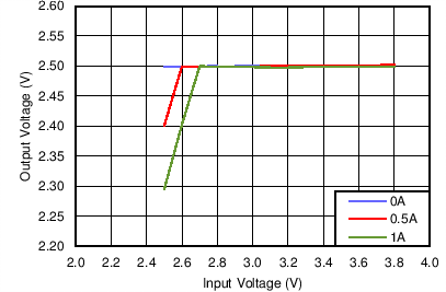
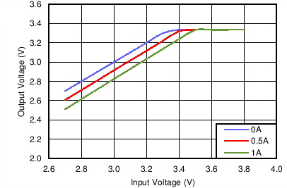
When the input voltage is close to the output voltage, the regulator will operate at very large duty cycles. Normal time delays of the internal circuits prevents the attainment of controlled duty cycles near 100%. In this condition, the LMZ20501 will skip switching cycles to maintain regulation with the highest possible input-to-output ratio. Some increase in output voltage ripple can appear as the regulator skips cycles. As the input voltage gets closer to the output voltage, the regulator will eventually reach 100% duty cycle, with the high side switch turned on. The output will then follow the input voltage minus the drop across the high-side switch and inductor resistance. Figure 7-5 and Figure 7-6 show typical dropout behavior for output voltages of 2.5 V and 3.3 V.
Since the internal gate drive levels of the LMZ20501 are dependent on input voltage, the Rdson of the power FETs will increase at low input voltages. This will result in degraded efficiency at input voltages below approximately 2.9 V. Also, combinations of low input voltage and high output voltage increase the effective switch duty cycle, which can result in increased output voltage ripple.
 Figure 7-5 Typical Dropout Behavior,
VOUT = 2.5 V
 Figure 7-6 Typical Dropout Behavior,
VOUT = 3.3 V