SLVSBM9E October 2013 – September 2018 LMZ31520
PRODUCTION DATA.
- 1 Features
- 2 Applications
- 3 Description
- 4 Specifications
- 5 Device Information
- 6 Typical Characteristics (PVIN = VIN = 12 V)
- 7 Typical Characteristics (PVIN = VIN = 5 V)
-
8 Application Information
- 8.1 Adjusting the Output Voltage
- 8.2 Frequency Select
- 8.3 Capacitor Recommendations for the LMZ31520 Power Supply
- 8.4 Transient Response
- 8.5 Application Curves Device configured for FCCM mode of operation, (pin 3 connected to pin 19).
- 8.6 Application Schematics
- 8.7 Custom Design With WEBENCH® Tools
- 8.8 VIN and PVIN Input Voltage
- 8.9 3.3 V PVIN Operation
- 8.10 Power Good (PWRGD)
- 8.11 Slow Start (SS_SEL)
- 8.12 Auto-Skip Eco-mode / Forced Continuous Conduction Mode
- 8.13 Power-Up Characteristics
- 8.14 Pre-Biased Start-Up
- 8.15 Remote Sense
- 8.16 Output On/Off Inhibit (INH)
- 8.17 Overcurrent Protection
- 8.18 Current Limit (ILIM) Adjust
- 8.19 Thermal Shutdown
- 8.20 Layout Considerations
- 8.21 EMI
- 9 Revision History
- 10Device and Documentation Support
- 11Mechanical, Packaging, and Orderable Information
Package Options
Refer to the PDF data sheet for device specific package drawings
Mechanical Data (Package|Pins)
- RLG|72
Thermal pad, mechanical data (Package|Pins)
Orderable Information
8.11 Slow Start (SS_SEL)
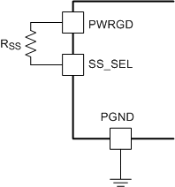
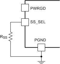
Connecting the SS_SEL pin to PWRGD or PGND sets the slow start interval of approximately 0.7 ms. The connection to either PWRGD or PGND determines the mode of the LMZ31520 as decribed in Auto-Skip Eco-mode / Forced Continuous Conduction Mode. Adding a resistor between SS_SEL pin and PWRGD or PGND increases the slow start time. Increasing the slow start time will reduce inrush current.Table 5 shows a resistor connected between SS_SEL pin and PWRGD to select FCCM and Figure 17 shows a resistor between SS_SEL pin and PGND to select Auto-skip mode. See Table 5 below for SS resistor values and timing interval.
 Figure 16. Slow-Start Resistor (RSS) in FCCM
  Figure 17. Slow-Start Resistor (RSS) in Auto-skip Mode
 Table 5. Slow-Start Resistor Values and Slow-Start Time
| RSS (kΩ) | short | 61.9 | 161 | 436 |
|---|---|---|---|---|
| SS Time (msec) | 0.7 | 1.4 | 2.8 | 5.6 |