SLVSBM9E October 2013 – September 2018 LMZ31520
PRODUCTION DATA.
- 1 Features
- 2 Applications
- 3 Description
- 4 Specifications
- 5 Device Information
- 6 Typical Characteristics (PVIN = VIN = 12 V)
- 7 Typical Characteristics (PVIN = VIN = 5 V)
-
8 Application Information
- 8.1 Adjusting the Output Voltage
- 8.2 Frequency Select
- 8.3 Capacitor Recommendations for the LMZ31520 Power Supply
- 8.4 Transient Response
- 8.5 Application Curves Device configured for FCCM mode of operation, (pin 3 connected to pin 19).
- 8.6 Application Schematics
- 8.7 Custom Design With WEBENCH® Tools
- 8.8 VIN and PVIN Input Voltage
- 8.9 3.3 V PVIN Operation
- 8.10 Power Good (PWRGD)
- 8.11 Slow Start (SS_SEL)
- 8.12 Auto-Skip Eco-mode / Forced Continuous Conduction Mode
- 8.13 Power-Up Characteristics
- 8.14 Pre-Biased Start-Up
- 8.15 Remote Sense
- 8.16 Output On/Off Inhibit (INH)
- 8.17 Overcurrent Protection
- 8.18 Current Limit (ILIM) Adjust
- 8.19 Thermal Shutdown
- 8.20 Layout Considerations
- 8.21 EMI
- 9 Revision History
- 10Device and Documentation Support
- 11Mechanical, Packaging, and Orderable Information
Package Options
Refer to the PDF data sheet for device specific package drawings
Mechanical Data (Package|Pins)
- RLG|72
Thermal pad, mechanical data (Package|Pins)
Orderable Information
6 Typical Characteristics (PVIN = VIN = 12 V)
The electrical characteristic data has been developed from actual products tested at 25°C. This data is considered typical for the converter. Applies to Figure 1, Figure 2, and Figure 3. The temperature derating curves represent the conditions at which internal components are at or below the manufacturer's maximum operating temperatures. Derating limits apply to devices soldered directly to a 100 mm × 100 mm six-layer PCB with 1 oz. copper. Applies to Figure 4 and Figure 5.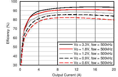 Figure 1. Efficiency vs. Output Current
 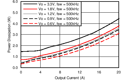 Figure 3. Power Dissipation vs. Output Current
 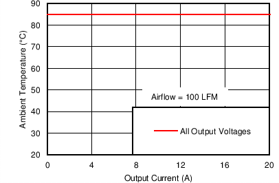 Figure 5. Safe Operating Area (100 LFM)
 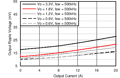 Figure 2. Voltage Ripple vs. Output Current
 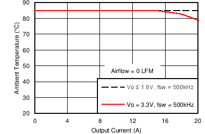 Figure 4. Safe Operating Area (0 LFM)