SNVSAQ4C December   2017  – March 2023 LMZM23601

PRODUCTION DATA  

  1. Features
  2. Applications
  3. Description
  4. Revision History
    1.     Device Comparison
  5. Pin Configuration and Functions
  6. Specifications
    1. 6.1 Absolute Maximum Ratings
    2. 6.2 ESD Ratings
    3. 6.3 Recommended Operating Conditions
    4. 6.4 Thermal Information
    5. 6.5 Electrical Characteristics
    6. 6.6 System Characteristics
    7. 6.7 Typical Characteristics
  7. Detailed Description
    1. 7.1 Overview
    2. 7.2 Functional Block Diagram
    3. 7.3 Feature Description
      1. 7.3.1 Control Scheme
      2. 7.3.2 Soft-Start Function
      3. 7.3.3 Enable and External UVLO Function
      4. 7.3.4 Current Limit
      5. 7.3.5 Hiccup Mode
      6. 7.3.6 Power Good (PGOOD) Function
      7. 7.3.7 MODE/SYNC Function
        1. 7.3.7.1 Forced PWM Mode
        2. 7.3.7.2 Auto PFM Mode
        3. 7.3.7.3 Dropout Mode
        4. 7.3.7.4 SYNC Operation
      8. 7.3.8 Thermal Protection
    4. 7.4 Device Functional Modes
      1. 7.4.1 Shutdown
      2. 7.4.2 FPWM Operation
      3. 7.4.3 Auto PFM Mode Operation
  8. Application and Implementation
    1. 8.1 Application Information
    2. 8.2 Typical Applications
      1. 8.2.1 Design Requirements
        1. 8.2.1.1 Maximum Input Voltage for VOUT < 2.5 V
      2. 8.2.2 Detailed Design Procedure
        1. 8.2.2.1 Custom Design With WEBENCH® Tools
        2. 8.2.2.2 Input Capacitor Selection
        3. 8.2.2.3 Output Capacitor Selection
        4. 8.2.2.4 Feedback Voltage Divider for Adjustable Output Voltage Versions
        5. 8.2.2.5 RPU - PGOOD Pullup Resistor
        6. 8.2.2.6 VIN Divider and Enable
      3. 8.2.3 Application Curves
        1. 8.2.3.1 VOUT = 5 V
        2. 8.2.3.2 VOUT = 3.3 V
        3. 8.2.3.3 VOUT = 12 V
        4. 8.2.3.4 VOUT = 15 V
        5. 8.2.3.5 VOUT = 2.5 V
        6. 8.2.3.6 VOUT = 1.2 V and VOUT = 1.8 V
        7. 8.2.3.7 VOUT = 5 V and 3.3 V Fixed Output Options
    3. 8.3 Best Design Practices
    4. 8.4 Power Supply Recommendations
      1. 8.4.1 Supply Voltage Range
      2. 8.4.2 Supply Current Capability
      3. 8.4.3 Supply Input Connections
        1. 8.4.3.1 Voltage Drops
        2. 8.4.3.2 Stability
    5. 8.5 Layout
      1. 8.5.1 Layout Guidelines
        1. 8.5.1.1 Thermal Design
      2. 8.5.2 Layout Examples
  9. Device and Documentation Support
    1. 9.1 Device Support
      1. 9.1.1 Third-Party Products Disclaimer
      2. 9.1.2 Development Support
        1. 9.1.2.1 Custom Design With WEBENCH® Tools
    2. 9.2 Documentation Support
      1. 9.2.1 Related Documentation
    3. 9.3 Receiving Notification of Documentation Updates
    4. 9.4 Support Resources
    5. 9.5 Trademarks
    6. 9.6 Electrostatic Discharge Caution
    7. 9.7 Glossary
  10. 10Mechanical, Packaging, and Orderable Information
    1. 10.1 Tape and Reel Information

Package Options

Refer to the PDF data sheet for device specific package drawings

Mechanical Data (Package|Pins)
  • SIL|10
Thermal pad, mechanical data (Package|Pins)
Orderable Information

Thermal Design

Thermal design is an important aspect of any power regulator design. Every supply dissipates some power, and providing sufficient copper area for proper heat dissipation is important. The package thermal resistance curves vs PCB copper area along with the power dissipation curves in GUID-CE8EB451-1634-4063-9734-9C45FBC8CE23.html#GUID-CE8EB451-1634-4063-9734-9C45FBC8CE23 can be used to estimate the necessary copper area for the design. Consider #X2806 and #X6004.

Equation 7. GUID-55B8DC0E-54FF-49F1-A362-6AFFC8724331-low.gif
GUID-2EE746D4-5FCE-4B1E-9B6B-CEC6FBC4237D-low.gif
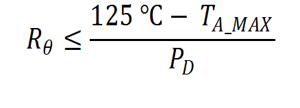
Figure 8-48 Package Thermal Resistance vs Board Copper Area

As an example, consider a typical application of 24-V input 5-V output with 0.8 A of output current and estimate the required heat-sinking area. For this example consider a maximum ambient temperature TA_MAX of 75°C and no air flow or additional heat sinking besides the PCB layers. Calculate the maximum allowed package thermal resistance for this design specification.

From GUID-CE8EB451-1634-4063-9734-9C45FBC8CE23.html#GUID-CE8EB451-1634-4063-9734-9C45FBC8CE23, it can be seen that the power dissipation for 24-V input, 5-V output, and 0.8A load is 0.75 W. Based on #X2806, for this power dissipation level and 75°C maximum ambient temperature, the maximum package thermal resistance must be less than 66.7°C/W. To achieve this thermal resistance with a 2-layer board, the approximate area of the board copper must be at least 9 cm2.