SNVSAO4D December 2017 – August 2020 LMZM33602
PRODUCTION DATA
- 1Features
- 2Applications
- 3Description
- 4Revision History
- 5Pin Configuration and Functions
- 6Specifications
-
7Detailed Description
- 7.1 Overview
- 7.2 Functional Block Diagram
- 7.3
Feature Description
- 7.3.1 Adjusting the Output Voltage
- 7.3.2 Feedforward Capacitor, CFF
- 7.3.3 Voltage Dropout
- 7.3.4 Switching Frequency (RT)
- 7.3.5 Synchronization (SYNC)
- 7.3.6 Input Capacitors
- 7.3.7 Output Capacitors
- 7.3.8 Output On/Off Enable (EN)
- 7.3.9 Programmable Undervoltage Lockout (UVLO)
- 7.3.10 Power Good (PGOOD)
- 7.3.11 Overcurrent Protection (OCP)
- 7.3.12 Thermal Shutdown
- 7.4 Device Functional Modes
- 8Application and Implementation
- 9Device and Documentation Support
Package Options
Mechanical Data (Package|Pins)
- RLR|18
Thermal pad, mechanical data (Package|Pins)
Orderable Information
7.3.8 Output On/Off Enable (EN)
The voltage on the EN/SYNC pin provides electrical ON/OFF control of the device. Once the EN pin voltage exceeds the threshold voltage, the device starts operation. If the EN pin voltage is pulled below the threshold voltage, the regulator stops switching and enters low quiescent current state.
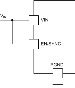
The EN pin cannot be open circuit or floating. The simplest way to enable the operation of the LMZM33602 is to connect the EN pin to VIN directly as shown in Figure 7-9. This allows self-start-up of the LMZM33602 when VIN is within the operation range.
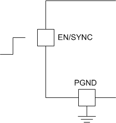
If an application requires controlling the EN pin, an external logic signal can be used to drive EN/SYNC pin as shown in Figure 7-10. Applications using an open drain/collector device to interface with this pin require a pullup resistor to a voltage above the enable threshold.
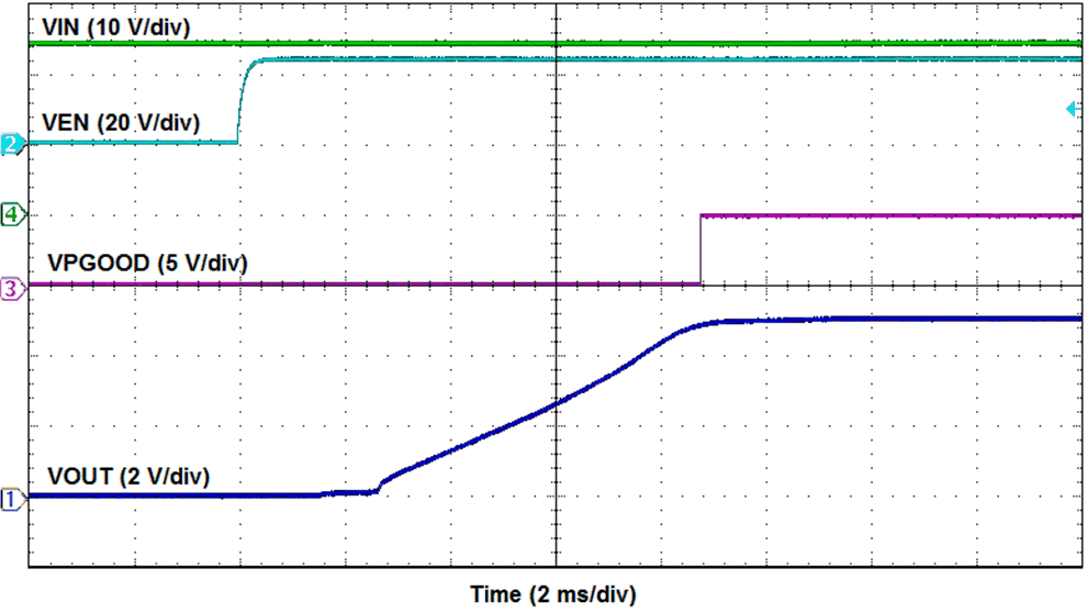
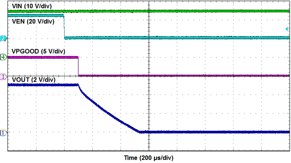
Figure 7-11 and Figure 7-12 show typical turn-ON and turn-OFF waveforms using the enable control.
 Figure 7-9 Enabling the Device
 Figure 7-10 Typical Enable Control
 Figure 7-11 Enable Turn-ON
 Figure 7-12 Enable Turn-OFF