SNVSAO6C September 2017 – March 2018 LMZM33603
PRODUCTION DATA.
- 1 Features
- 2 Applications
- 3 Description
- 4 Revision History
- 5 Pin Configuration and Functions
- 6 Specifications
-
7 Detailed Description
- 7.1 Overview
- 7.2 Functional Block Diagram
- 7.3
Feature Description
- 7.3.1 Adjusting the Output Voltage
- 7.3.2 Feed-Forward Capacitor, CFF
- 7.3.3 Output Current vs Output Voltage
- 7.3.4 Voltage Dropout
- 7.3.5 Switching Frequency (RT)
- 7.3.6 Synchronization (SYNC)
- 7.3.7 Input Capacitors
- 7.3.8 Output Capacitors
- 7.3.9 Output On/Off Enable (EN)
- 7.3.10 Programmable Undervoltage Lockout (UVLO)
- 7.3.11 Power Good (PGOOD)
- 7.3.12 Overcurrent Protection (OCP)
- 7.3.13 Thermal Shutdown
- 7.4 Device Functional Modes
- 8 Application and Implementation
- 9 Power Supply Recommendations
- 10Layout
- 11Device and Documentation Support
- 12Mechanical, Packaging, and Orderable Information
Package Options
Mechanical Data (Package|Pins)
- RLR|18
Thermal pad, mechanical data (Package|Pins)
Orderable Information
10.3 Theta JA vs PCB Area
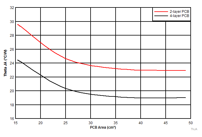
The amount of PCB copper effects the thermal performance of the device. Figure 42 shows the effects of copper area on the junction-to-ambient thermal resistance (RθJA) of the LMZM33603. The junction-to-ambient thermal resistance is plotted for a 2-layer PCB and a 4-layer PCB with PCB area from 16 cm2 to 49 cm2.
To determine the required copper area for an application:
- Determine the maximum power dissipation of the device in the application by referencing the power dissipation graphs in the Typical Characteristics section.
- Calculate the maximum θJA using Equation 5 and the maximum ambient temperature of the application.
- Reference Figure 42 to determine the minimum required PCB area for the application conditions.
Equation 5. 

 Figure 42. θJA vs PCB Area