SNVSAO6C September   2017  – March 2018 LMZM33603

PRODUCTION DATA.  

  1. Features
  2. Applications
    1.     Simplified Schematic
  3. Description
    1.     Safe Operating Area
  4. Revision History
  5. Pin Configuration and Functions
    1.     Pin Functions
  6. Specifications
    1. 6.1 Absolute Maximum Ratings
    2. 6.2 ESD Ratings
    3. 6.3 Recommended Operating Conditions
    4. 6.4 Thermal Information
    5. 6.5 Electrical Characteristics
    6. 6.6 Switching Characteristics
    7. 6.7 Typical Characteristics (VIN = 5 V)
    8. 6.8 Typical Characteristics (VIN = 12 V)
    9. 6.9 Typical Characteristics (VIN = 24 V)
  7. Detailed Description
    1. 7.1 Overview
    2. 7.2 Functional Block Diagram
    3. 7.3 Feature Description
      1. 7.3.1  Adjusting the Output Voltage
      2. 7.3.2  Feed-Forward Capacitor, CFF
      3. 7.3.3  Output Current vs Output Voltage
      4. 7.3.4  Voltage Dropout
      5. 7.3.5  Switching Frequency (RT)
      6. 7.3.6  Synchronization (SYNC)
      7. 7.3.7  Input Capacitors
      8. 7.3.8  Output Capacitors
      9. 7.3.9  Output On/Off Enable (EN)
      10. 7.3.10 Programmable Undervoltage Lockout (UVLO)
      11. 7.3.11 Power Good (PGOOD)
      12. 7.3.12 Overcurrent Protection (OCP)
      13. 7.3.13 Thermal Shutdown
    4. 7.4 Device Functional Modes
      1. 7.4.1 Active Mode
      2. 7.4.2 Shutdown Mode
  8. Application and Implementation
    1. 8.1 Application Information
    2. 8.2 Typical Application
      1. 8.2.1 Design Requirements
      2. 8.2.2 Detailed Design Procedure
        1. 8.2.2.1 Custom Design With WEBENCH® Tools
        2. 8.2.2.2 Output Voltage Setpoint
        3. 8.2.2.3 Feed-Forward Capacitor (CFF)
        4. 8.2.2.4 Setting the Switching Frequency
        5. 8.2.2.5 Input Capacitors
        6. 8.2.2.6 Output Capacitor Selection
        7. 8.2.2.7 Application Curves
  9. Power Supply Recommendations
  10. 10Layout
    1. 10.1 Layout Guidelines
    2. 10.2 Layout Examples
    3. 10.3 Theta JA vs PCB Area
    4. 10.4 EMI
      1. 10.4.1 EMI Plots
    5. 10.5 Package Specifications
  11. 11Device and Documentation Support
    1. 11.1 Device Support
      1. 11.1.1 Third-Party Products Disclaimer
      2. 11.1.2 Custom Design With WEBENCH® Tools
    2. 11.2 Related Documentation
    3. 11.3 Receiving Notification of Documentation Updates
    4. 11.4 Community Resources
    5. 11.5 Trademarks
    6. 11.6 Electrostatic Discharge Caution
    7. 11.7 Glossary
  12. 12Mechanical, Packaging, and Orderable Information
    1. 12.1 Tape and Reel Information

Package Options

Mechanical Data (Package|Pins)
Thermal pad, mechanical data (Package|Pins)
Orderable Information

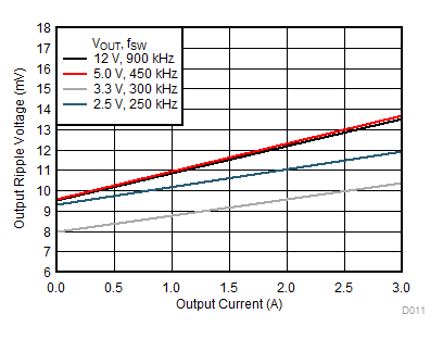
Typical Characteristics (VIN = 24 V)

The typical characteristic data has been developed from actual products tested at 25°C. This data is considered typical for the device.
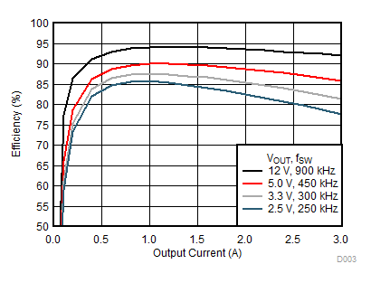
LMZM33603 24VEff_SNVSA06.gif
Figure 12. Efficiency vs Output Current
LMZM33603 D011w1Va.gif
COUT = 4 × 22 µF, 25 V, 1210 ceramic
Figure 14. Voltage Ripple vs Output Current
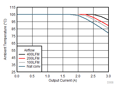
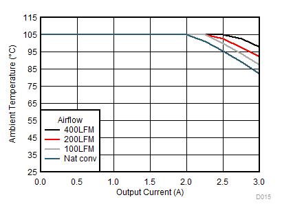
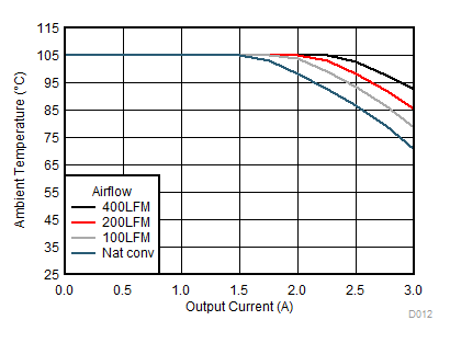
LMZM33603 SOA24to5V.gif
VOUT = 5 V fSW = 450 kHz
Figure 16. Safe Operating Area
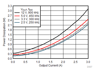
LMZM33603 24VPdis_SNVSA06.gif
Figure 13. Power Dissipation vs Output Current
LMZM33603 SOA24to33V.gif
VOUT = 3.3 V fSW = 300 kHz
Figure 15. Safe Operating Area
LMZM33603 SOA24to12V.gif
VOUT = 12 V fSW = 900 kHz
Figure 17. Safe Operating Area