SLVS582I April 2006 – November 2014 LP2950 , LP2951
PRODUCTION DATA.
- 1 Features
- 2 Applications
- 3 Description
- 4 Revision History
- 5 Pin Configuration and Functions
- 6 Specifications
- 7 Detailed Description
- 8 Application and Implementation
- 9 Power Supply Recommendations
- 10Layout
- 11Device and Documentation Support
- 12Mechanical, Packaging, and Orderable Information
Package Options
Mechanical Data (Package|Pins)
Thermal pad, mechanical data (Package|Pins)
- DRG|8
Orderable Information
6 Specifications
6.1 Absolute Maximum Ratings
over operating free-air temperature range (unless otherwise noted) (1)| MIN | MAX | UNIT | ||
|---|---|---|---|---|
| VIN | Continuous input voltage range | –0.3 | 30 | V |
| VSHDN | SHUTDOWN input voltage range | –1.5 | 30 | V |
| VERROR | ERROR comparator output voltage range(2) | –1.5 | 30 | V |
| VFDBK | FEEDBACK input voltage range(2)(3) | –1.5 | 30 | V |
(1) Stresses beyond those listed under Absolute Maximum Ratings may cause permanent damage to the device. These are stress ratings only, which do not imply functional operation of the device at these or any other conditions beyond those indicated under Recommended Operating Conditions. Exposure to absolute-maximum-rated conditions for extended periods may affect device reliability.
(2) May exceed input supply voltage
(3) If load is returned to a negative power supply, the output must be diode clamped to GND.
6.2 Handling Ratings
| MIN | MAX | UNIT | |||
|---|---|---|---|---|---|
| Tstg | Storage temperature range | –65 | 150 | °C | |
| V(ESD) | Electrostatic discharge | Human body model (HBM), per ANSI/ESDA/JEDEC JS-001, all pins(1) | 0 | 2500 | V |
| Charged device model (CDM), per JEDEC specification JESD22-C101, all pins(2) | 0 | 1000 | |||
(1) JEDEC document JEP155 states that 500-V HBM allows safe manufacturing with a standard ESD control process.
(2) JEDEC document JEP157 states that 250-V CDM allows safe manufacturing with a standard ESD control process.
6.3 Recommended Operating Conditions
| MIN | MAX | UNIT | ||
|---|---|---|---|---|
| VIN | Supply input voltage | See (1) | 30 | V |
| TJ | Operating virtual junction temperature | –40 | 125 | °C |
(1) Minimum VIN is the greater of:
- 2 V (25°C), 2.3 V (over temperature), or
- VOUT(MAX) + Dropout (Max) at rated IL
6.4 Thermal Information
| THERMAL METRIC(1) | LP2950 | LP2951 | UNIT | |||
|---|---|---|---|---|---|---|
| LP | D | P | DRG | |||
| 3 PINS | 8 PINS | |||||
| RθJA | Junction-to-ambient thermal resistance | 140 | 97 | 84.6 | 52.44 | °C/W |
(1) For more information about traditional and new thermal metrics, see the IC Package Thermal Metrics application report (SPRA953).
6.5 Electrical Characteristics
VIN = VOUT (nominal) + 1 V, IL = 100 μA, CL = 1 μF (5-V versions) or CL = 2.2 μF (3-V and 3.3-V versions),8-pin version: FEEDBACK tied to VTAP, OUTPUT tied to SENSE, VSHUTDOWN ≤ 0.7 V
| PARAMETER | TEST CONDITIONS | TJ | MIN | TYP | MAX | UNIT | |
|---|---|---|---|---|---|---|---|
| 3-V VERSION (LP295x-30) | |||||||
| VOUT | Output voltage | IL = 100 μA | 25°C | 2.970 | 3 | 3.030 | V |
| –40°C to 125°C | 2.940 | 3 | 3.060 | ||||
| 3.3-V VERSION (LP295x-33) | |||||||
| VOUT | Output voltage | IL = 100 μA | 25°C | 3.267 | 3.3 | 3.333 | V |
| –40°C to 125°C | 3.234 | 3.3 | 3.366 | ||||
| 5-V VERSION (LP295x-50) | |||||||
| VOUT | Output voltage | IL = 100 μA | 25°C | 4.950 | 5 | 5.050 | V |
| –40°C to 125°C | 4.900 | 5 | 5.100 | ||||
| ALL VOLTAGE OPTIONS | |||||||
| Output voltage temperature coefficient(1) | IL = 100 μA | –40°C to 125°C | 20 | 100 | ppm/°C | ||
| Line regulation(2) | VIN = [VOUT(NOM) + 1 V] to 30 V | 25°C | 0.03 | 0.2 | %/V | ||
| –40°C to 125°C | 0.4 | ||||||
| Load regulation(2) | IL = 100 μA to 100 mA | 25°C | 0.04% | 0.2% | — | ||
| –40°C to 125°C | 0.3% | ||||||
| VIN – VOUT | Dropout voltage(3) | IL = 100 μA | 25°C | 50 | 80 | mV | |
| –40°C to 125°C | 150 | ||||||
| IL = 100 mA | 25°C | 380 | 450 | ||||
| –40°C to 125°C | 600 | ||||||
| IGND | GND current | IL = 100 μA | 25°C | 75 | 120 | μA | |
| –40°C to 125°C | 140 | ||||||
| IL = 100 mA | 25°C | 8 | 12 | mA | |||
| –40°C to 125°C | 14 | ||||||
| Dropout ground current | VIN = VOUT(NOM) – 0.5 V, IL = 100 μA |
25°C | 110 | 170 | μA | ||
| –40°C to 125°C | 200 | ||||||
| Current limit | VOUT = 0 V | 25°C | 160 | 200 | mA | ||
| –40°C to 125°C | 220 | ||||||
| Thermal regulation(4) | IL = 100 μA | 25°C | 0.05 | 0.2 | %/W | ||
| Output noise (RMS), 10 Hz to 100 kHz |
CL = 1 μF (5 V only) | 25°C | 430 | μV | |||
| CL = 200 μF | 160 | ||||||
| LP2951-50: CL = 3.3 μF, CBypass = 0.01 μF between pins 1 and 7 |
100 | ||||||
| (LP2951-xx) 8-PIN VERSION ONLY ADJ | |||||||
| Reference voltage | 25°C | 1.218 | 1.235 | 1.252 | V | ||
| –40°C to 125°C | 1.212 | 1.257 | |||||
| VOUT = VREF to (VIN – 1 V), VIN = 2.3 V to 30 V, IL = 100 μA to 100 mA |
–40°C to 125°C | 1.200 | 1.272 | ||||
| Reference voltage temperature coefficient(1) | 25°C | 20 | ppm/°C | ||||
| FEEDBACK bias current | 25°C | 20 | 40 | nA | |||
| –40°C to 125°C | 60 | ||||||
| FEEDBACK bias current temperature coefficient | 25°C | 0.1 | nA/°C | ||||
| ERROR COMPARATOR | |||||||
| Output leakage current | VOUT = 30 V | 25°C | 0.01 | 1 | μA | ||
| –40°C to 125°C | 2 | ||||||
| Output low voltage | VIN = VOUT(NOM) – 0.5 V, IOL = 400 μA |
25°C | 150 | 250 | mV | ||
| –40°C to 125°C | 400 | ||||||
| Upper threshold voltage (ERROR output high)(5) | 25°C | 40 | 60 | mV | |||
| –40°C to 125°C | 25 | ||||||
| Lower threshold voltage (ERROR output low)(5) | 25°C | 75 | 95 | mV | |||
| –40°C to 125°C | 140 | ||||||
| Hysteresis(5) | 25°C | 15 | mV | ||||
| SHUTDOWN INPUT | |||||||
| Input logic voltage | Low (regulator ON) | –40°C to 125°C | 0.7 | V | |||
| High (regulator OFF) | 2 | ||||||
| SHUTDOWN input current | SHUTDOWN = 2.4 V | 25°C | 30 | 50 | μA | ||
| –40°C to 125°C | 100 | ||||||
| SHUTDOWN = 30 V | 25°C | 450 | 600 | ||||
| –40°C to 125°C | 750 | ||||||
| Regulator output current in shutdown |
VSHUTDOWN ≥ 2 V, VIN ≤ 30 V, VOUT = 0, FEEDBACK tied to VTAP |
25°C | 3 | 10 | μA | ||
| –40°C to 125°C | 20 | ||||||
(1) Output or reference voltage temperature coefficient is defined as the worst-case voltage change divided by the total temperature range.
(2) Regulation is measured at constant junction temperature, using pulse testing with a low duty cycle. Changes in output voltage due to heating effects are covered under the specification for thermal regulation.
(3) Dropout voltage is defined as the input-to-output differential at which the output voltage drops 100 mV, below the value measured at 1-V differential. The minimum input supply voltage of 2 V (2.3 V over temperature) must be observed.
(4) Thermal regulation is defined as the change in output voltage at a time (T) after a change in power dissipation is applied, excluding load or line regulation effects. Specifications are for a 50-mA load pulse at VIN = 30 V, VOUT = 5 V (1.25-W pulse) for t = 10 ms.
(5) Comparator thresholds are expressed in terms of a voltage differential equal to the nominal reference voltage (measured at VIN – VOUT = 1 V) minus FEEDBACK terminal voltage. To express these thresholds in terms of output voltage change, multiply by the error amplifier gain = VOUT/VREF = (R1 + R2)/R2. For example, at a programmed output voltage of 5 V, the ERROR output is specified to go low when the output drops by 95 mV × 5 V/1.235 V = 384 mV. Thresholds remain constant as a percentage of VOUT (as VOUT is varied), with the low-output warning occurring at 6% below nominal (typ) and 7.7% (max).
6.6 Typical Characteristics
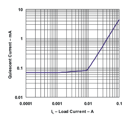 Figure 1. Quiescent Current vs Load Current
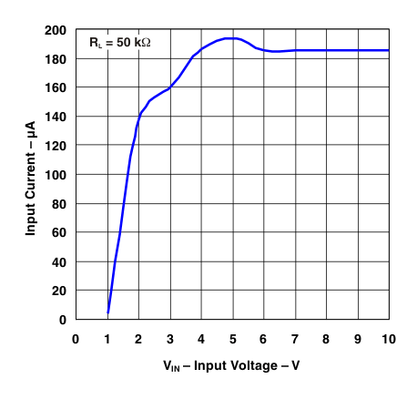 Figure 3. Input Current vs Input Voltage (RL = 50 kΩ)
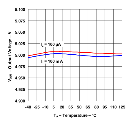 Figure 5. Output Voltage vs Temperature
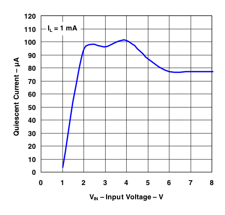 Figure 7. Quiescent Current vs Input Voltage (IL = 1 mA)
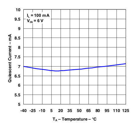 Figure 9. Quiescent Current vs Temperature (IL = 100 mA)
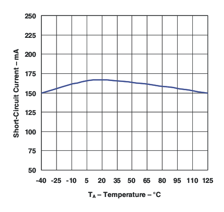 Figure 11. Short-circuit Current vs Temperature
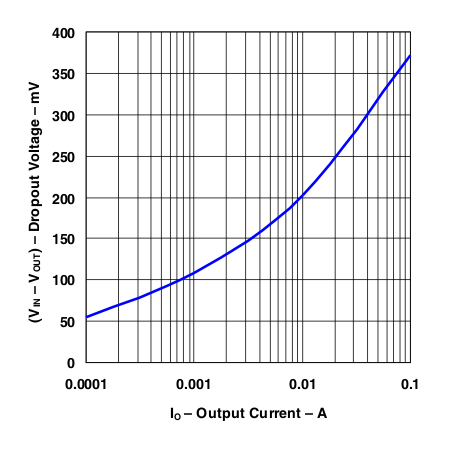 Figure 13. Dropout Voltage vs Dropout Current
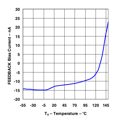 Figure 15. LP2951 FEEDBACK Bias Current vs Temperature
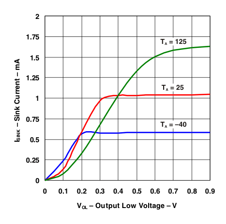 Figure 17. LP2951 ERROR Comparator Sink Current vs Output Low Voltage
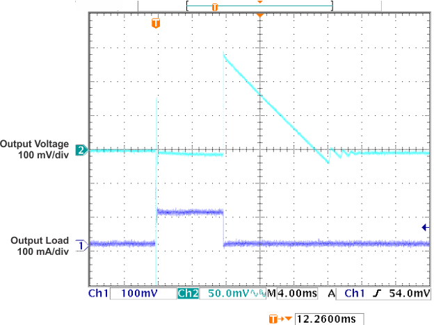 Figure 19. Load Transient Response vs
Time (VOUT = 5 V, CL = 10 µF)
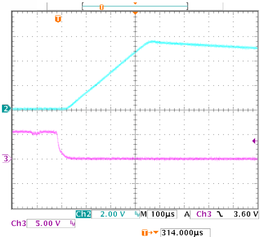 Figure 21. Enable Transient Response vs
Time (IL = 1 mA, CL = 10 µF)
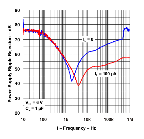 Figure 23. Ripple Rejection vs Frequency
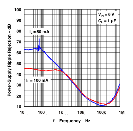 Figure 25. Output Impedance vs Frequency
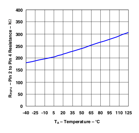 Figure 27. LP2951 Divider Resistance vs Temperature
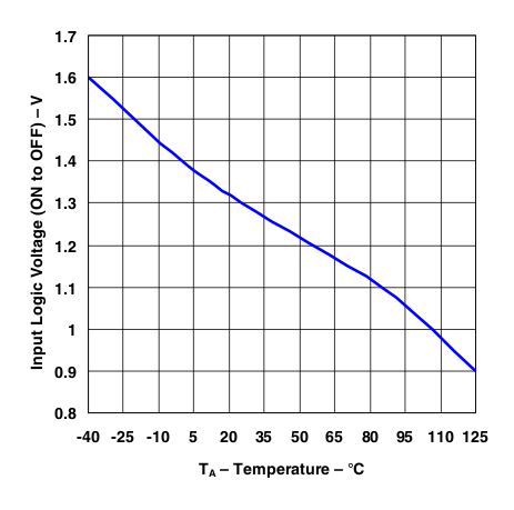 Figure 29. Shutdown Threshold Voltage (On to Off) vs Temperature
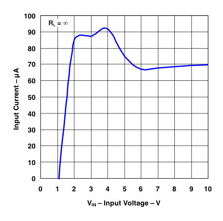 Figure 2. Input Current vs Input Voltage (RL = OPEN)
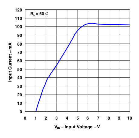 Figure 4. Input Current vs Input Voltage (RL = 50 Ω)
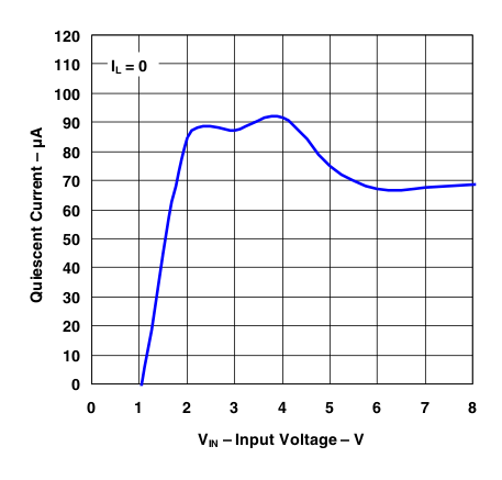 Figure 6. Quiescent Current vs Input Voltage (IL = 0)
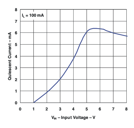 Figure 8. Quiescent Current vs Input Voltage (IL = 100 mA)
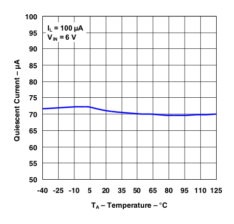 Figure 10. Quiescent Current vs Temperature (IL = 100 µA)
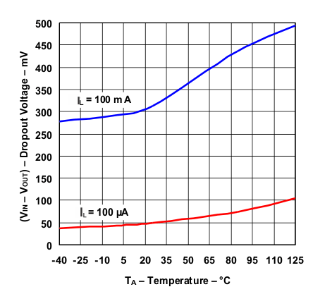 Figure 12. Dropout Voltage vs Temperature
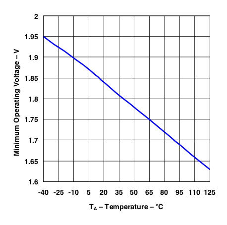 Figure 14. LP2951 Minimum Operating Voltage vs Temperature
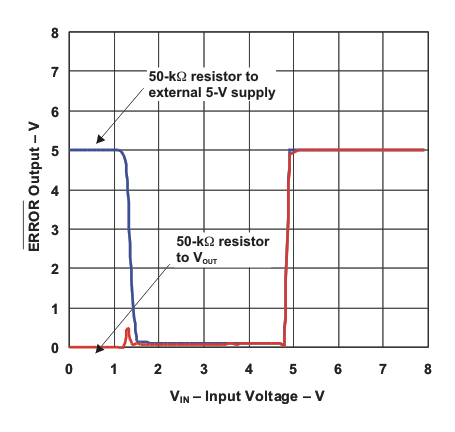 Figure 16. LP2951 ERROR Comparator Output vs
Input Voltage
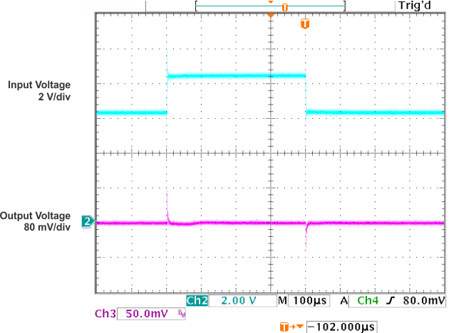 Figure 18. Line Transient Response vs Time
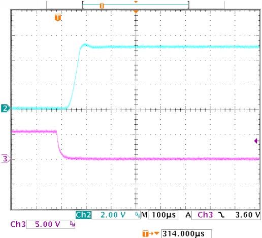 Figure 20. Enable Transient Response vs
Time (IL = 1 mA, CL = 1 µF)
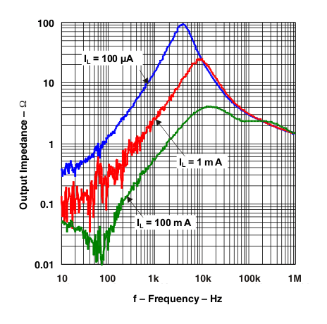 Figure 22. Output Impedance vs Frequency
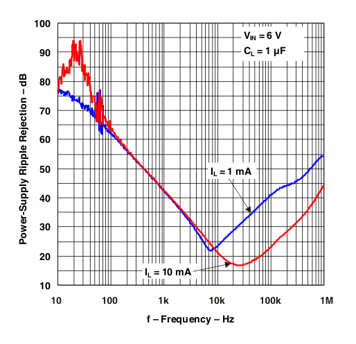 Figure 24. Output Impedance vs Frequency
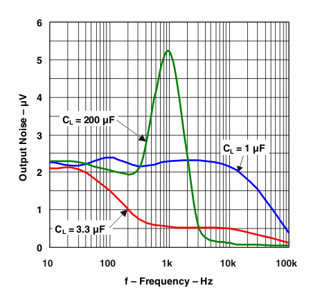 Figure 26. LP2951 Output Noise vs Frequency
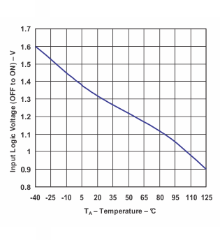 Figure 28. Shutdown Threshold Voltage (Off to On) vs Temperature
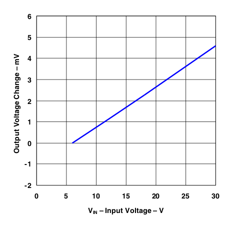 Figure 30. Line Regulation vs Input Voltage