SLVS522R july   2004  – july 2023 LP2985 , LP2985A

PRODUCTION DATA  

  1.   1
  2. Features
  3. Applications
  4. Description
  5. Revision History
  6. Pin Configuration and Functions
  7. Specifications
    1. 6.1 Absolute Maximum Ratings
    2. 6.2 ESD Ratings
    3. 6.3 Recommended Operating Conditions
    4. 6.4 Thermal Information
    5. 6.5 Electrical Characteristics
    6. 6.6 Typical Characteristics
  8. Detailed Description
    1. 7.1 Overview
    2. 7.2 Functional Block Diagram
    3. 7.3 Feature Description
      1. 7.3.1 Output Enable
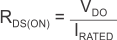
      2. 7.3.2 Dropout Voltage
      3. 7.3.3 Current Limit
      4. 7.3.4 Undervoltage Lockout (UVLO)
      5. 7.3.5 Output Pulldown
      6. 7.3.6 Thermal Shutdown
    4. 7.4 Device Functional Modes
      1. 7.4.1 Device Functional Mode Comparison
      2. 7.4.2 Normal Operation
      3. 7.4.3 Dropout Operation
      4. 7.4.4 Disabled
  9. Application and Implementation
    1. 8.1 Application Information
      1. 8.1.1 Recommended Capacitor Types
      2. 8.1.2 Input and Output Capacitor Requirements
      3. 8.1.3 Noise Bypass Capacitor (CBYPASS)
      4. 8.1.4 Reverse Current
      5. 8.1.5 Power Dissipation (PD)
      6. 8.1.6 Estimating Junction Temperature
    2. 8.2 Typical Application
      1. 8.2.1 Design Requirements
      2. 8.2.2 Detailed Design Procedure
        1. 8.2.2.1 ON/OFF Operation
      3. 8.2.3 Application Curves
    3. 8.3 Power Supply Recommendations
    4. 8.4 Layout
      1. 8.4.1 Layout Guidelines
      2. 8.4.2 Layout Example
  10. Device and Documentation Support
    1. 9.1 Device Nomenclature
    2. 9.2 Receiving Notification of Documentation Updates
    3. 9.3 Support Resources
    4. 9.4 Trademarks
    5. 9.5 Electrostatic Discharge Caution
    6. 9.6 Glossary
  11. 10Mechanical, Packaging, and Orderable Information

Package Options

Mechanical Data (Package|Pins)
Thermal pad, mechanical data (Package|Pins)
Orderable Information

Dropout Voltage

Dropout voltage (VDO) is defined as the input voltage minus the output voltage (VIN – VOUT) at the rated output current (IRATED), where the pass transistor is fully on. IRATED is the maximum IOUT listed in the Recommended Operating Conditions table. The pass transistor is in the ohmic or triode region of operation, and acts as a switch. The dropout voltage indirectly specifies a minimum input voltage greater than the nominal programmed output voltage at which the output voltage is expected to stay in regulation. If the input voltage falls to less than the nominal output regulation, then the output voltage falls as well.

For a CMOS regulator, the dropout voltage is determined by the drain-source on-state resistance (RDS(ON)) of the pass transistor. Therefore, if the linear regulator operates at less than the rated current, the dropout voltage for that current scales accordingly. The following equation calculates the RDS(ON) of the device.

Equation 1. GUID-17F79C89-58DF-409D-8C5A-45B06F6B258E-low.gif