SNVSAT4A September 2017 – June 2021 LP873220-Q1
PRODUCTION DATA
- 1 Features
- 2 Applications
- 3 Description
- 4 Revision History
- 5 Pin Configuration and Functions
- 6 Specifications
-
7 Detailed Description
- 7.1 Overview
- 7.2 Functional Block Diagram
- 7.3
Feature Description
- 7.3.1 DC/DC Converters
- 7.3.2 Sync Clock Functionality
- 7.3.3 Low-Dropout Linear Regulators (LDOs)
- 7.3.4 Power-Up
- 7.3.5 Regulator Control
- 7.3.6 Enable and Disable Sequences
- 7.3.7 Device Reset Scenarios
- 7.3.8 Diagnosis and Protection Features
- 7.3.9 Operation of the GPO Signals
- 7.3.10 Digital Signal Filtering
- 7.4 Device Functional Modes
- 7.5 Programming
- 7.6
Register Maps
- 7.6.1
Register Descriptions
- 7.6.1.1 DEV_REV
- 7.6.1.2 OTP_REV
- 7.6.1.3 BUCK0_CTRL_1
- 7.6.1.4 BUCK0_CTRL_2
- 7.6.1.5 BUCK1_CTRL_1
- 7.6.1.6 BUCK1_CTRL_2
- 7.6.1.7 BUCK0_VOUT
- 7.6.1.8 BUCK1_VOUT
- 7.6.1.9 LDO0_CTRL
- 7.6.1.10 LDO1_CTRL
- 7.6.1.11 LDO0_VOUT
- 7.6.1.12 LDO1_VOUT
- 7.6.1.13 BUCK0_DELAY
- 7.6.1.14 BUCK1_DELAY
- 7.6.1.15 LDO0_DELAY
- 7.6.1.16 LDO1_DELAY
- 7.6.1.17 GPO_DELAY
- 7.6.1.18 GPO2_DELAY
- 7.6.1.19 GPO_CTRL
- 7.6.1.20 CONFIG
- 7.6.1.21 PLL_CTRL
- 7.6.1.22 PGOOD_CTRL_1
- 7.6.1.23 PGOOD_CTRL_2
- 7.6.1.24 PG_FAULT
- 7.6.1.25 RESET
- 7.6.1.26 INT_TOP_1
- 7.6.1.27 INT_TOP_2
- 7.6.1.28 INT_BUCK
- 7.6.1.29 INT_LDO
- 7.6.1.30 TOP_STAT
- 7.6.1.31 BUCK_STAT
- 7.6.1.32 LDO_STAT
- 7.6.1.33 TOP_MASK_1
- 7.6.1.34 TOP_MASK_2
- 7.6.1.35 BUCK_MASK
- 7.6.1.36 LDO_MASK
- 7.6.1.37 SEL_I_LOAD
- 7.6.1.38 I_LOAD_2
- 7.6.1.39 I_LOAD_1
- 7.6.1
Register Descriptions
- 8 Application and Implementation
- 9 Power Supply Recommendations
- 10Layout
- 11Device and Documentation Support
- 12Mechanical, Packaging, and Orderable Information
Package Options
Mechanical Data (Package|Pins)
- RHD|28
Thermal pad, mechanical data (Package|Pins)
- RHD|28
Orderable Information
7.3.5.1 Enabling and Disabling Regulators
The regulators can be enabled when the device is in STANDBY or ACTIVE state. There are two ways to enable and disable the buck regulators:
- Using the BUCKx_EN bit in the BUCKx_CTRL_1 register (the BUCKx_EN_PIN_CTRL bit is 0 in the BUCKx_CTRL_1 register).
- Using the EN control pin (the BUCKx_EN bit and the BUCKx_EN_PIN_CTRL bit is 1).
Similarly, there are two ways to enable and disable the LDO regulators:
- Using the LDOx_EN bit in the LDOx_CTRL register (the LDOx_EN_PIN_CTRL bit is 0 in the LDOx_CTRL register).
- Using the EN control pin (the LDOx_EN bit is 1 and the LDOx_EN_PIN_CTRL bit is 1).
If the EN control pin is used for enable and disable, then the following occurs:
- The delay from the control signal rising edge to start-up is set by the BUCKx_STARTUP_DELAY[3:0] bits in the BUCKx_DELAY register and the LDOx_STARTUP_DELAY[3:0] bits in the LDOx_DELAY register.
- The delay from the control signal falling edge to shutdown is set by the BUCKx_SHUTDOWN_DELAY[3:0] bits in the BUCKx_DELAY register and the LDOx_SHUTDOWN_DELAY[3:0] bits in the LDOx_DELAY register.
The control of the regulator (with 0-ms delays) is shown in Table 7-3.
| BUCKx_EN AND LDOx_EN | BUCKx_EN_PIN_CTRL AND LDOx_EN_PIN_CTRL | EN PIN | BUCKx OUTPUT VOLTAGE AND LDOx OUTPUT VOLTAGE | |
|---|---|---|---|---|
| Enable and disable control with the BUCKx_EN and the LDOx_EN bit | 0 | Don't Care | Don't Care | Disabled |
| 1 | 0 | Don't Care | BUCKx_VSET[7:0] and LDOx_VSET[4:0] | |
| Enable and disable control with the EN pin | 1 | 1 | Low | Disabled |
| 1 | 1 | High | BUCKx_VSET[7:0] and LDOx_VSET[4:0] |
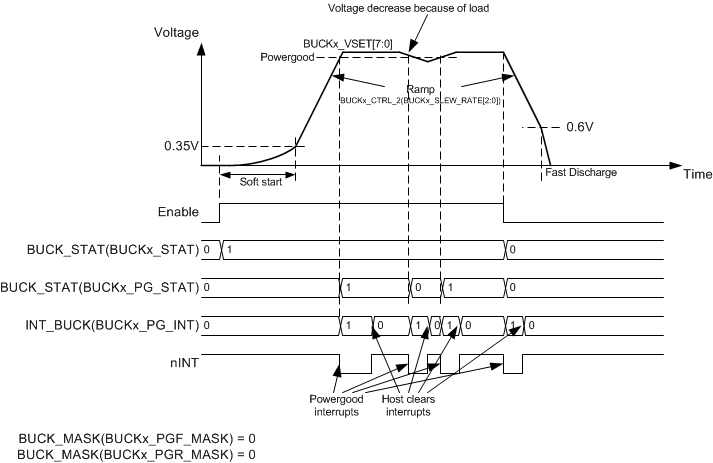
The buck regulator is enabled by the EN pin or by I2C writing as shown in Figure 7-4. The soft-start circuit limits the in-rush current during start-up. When the output voltage rises to a 0.35-V level, the output voltage becomes slew-rate controlled. If there is a short circuit at the output, and the output voltage does not increase above the 0.35-V level in 1 ms or the output voltage drops below 0.35-V level during operation (for minimum of 1 ms), then the regulator is disabled, and the BUCKx_SC_INT interrupt in the INT_BUCK register is set. When the output voltage reaches the Power-Good threshold level, the BUCKx_PG_INT interrupt flag in the INT_BUCK register is set. The Power-Good interrupt flag, when reaching valid output voltage, can be masked using the BUCKx_PGR_MASK bit in the BUCK_MASK register. The Power-Good interrupt flag can also be generated when the output voltage becomes invalid. The interrupt mask for invalid output voltage detection is set by the BUCKx_PGF_MASK bit in the BUCK_MASK register. A BUCKx_PG_STAT bit in the BUCK_STAT register always shows the validity of the output voltage; 1 means valid and 0 means invalid output voltage. A PGOOD_WINDOW_BUCK bit in the PGOOD_CTRL_1 register sets the detection method for the valid buck output voltage, either undervoltage detection or undervoltage and overvoltage detection.
 Figure 7-4 Buck Regulator Enable and Disable
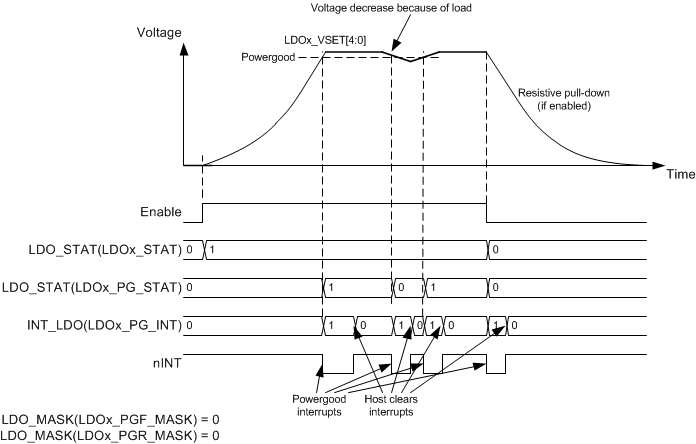
The LDO regulator is enabled by the EN pin or by I2C writing, as shown in Figure 7-5. The soft-start circuit limits the in-rush current during start-up. The output voltage increase rate is less than 100 mV/μsec during soft-start. If there is a short circuit at the output, and the output voltage does not increase above the 0.3-V level in 1 ms or the output voltage drops below 0.3-V level during operation (for minimum of 1 ms), then the regulator is disabled, and the LDOx_SC_INT interrupt in the INT_LDO register is set. When the output voltage reaches the Power-Good threshold level, the LDOx_PG_INT interrupt flag in the INT_LDO register is set. The Power-Good interrupt flag, when reaching valid output voltage, can be masked using the LDOx_PGR_MASK bit in the LDO_MASK register. The Power-Good interrupt flag can also be generated when the output voltage becomes invalid. The interrupt mask for invalid output voltage detection is set by the LDOx_PGF_MASK bit in the LDO_MASK register. A LDOx_PG_STAT bit in the LDO_STAT register always shows the validity of the output voltage; 1 means valid, and 0 means invalid output voltage. A PGOOD_WINDOW_LDO bit in the PGOOD_CTRL_1 register sets the detection method for the valid LDO output voltage, either undervoltage detection or undervoltage and overvoltage detection.
 Figure 7-5 LDO Regulator Enable and Disable
The EN input pin has an integrated pulldown resistor. The pulldown resistor is controlled with the EN_PD bit in the CONFIG register.